Email alert
 RSS
RSS2024 Vol. 36, No. 2
Recommend Articles
column
Display Method:
2024,
36: 1-2.
2024,
36: 025001.
doi: 10.11884/HPLPB202436.230241
Abstract:
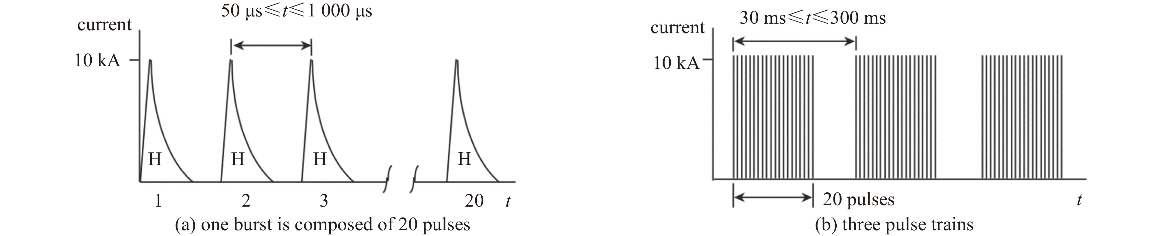
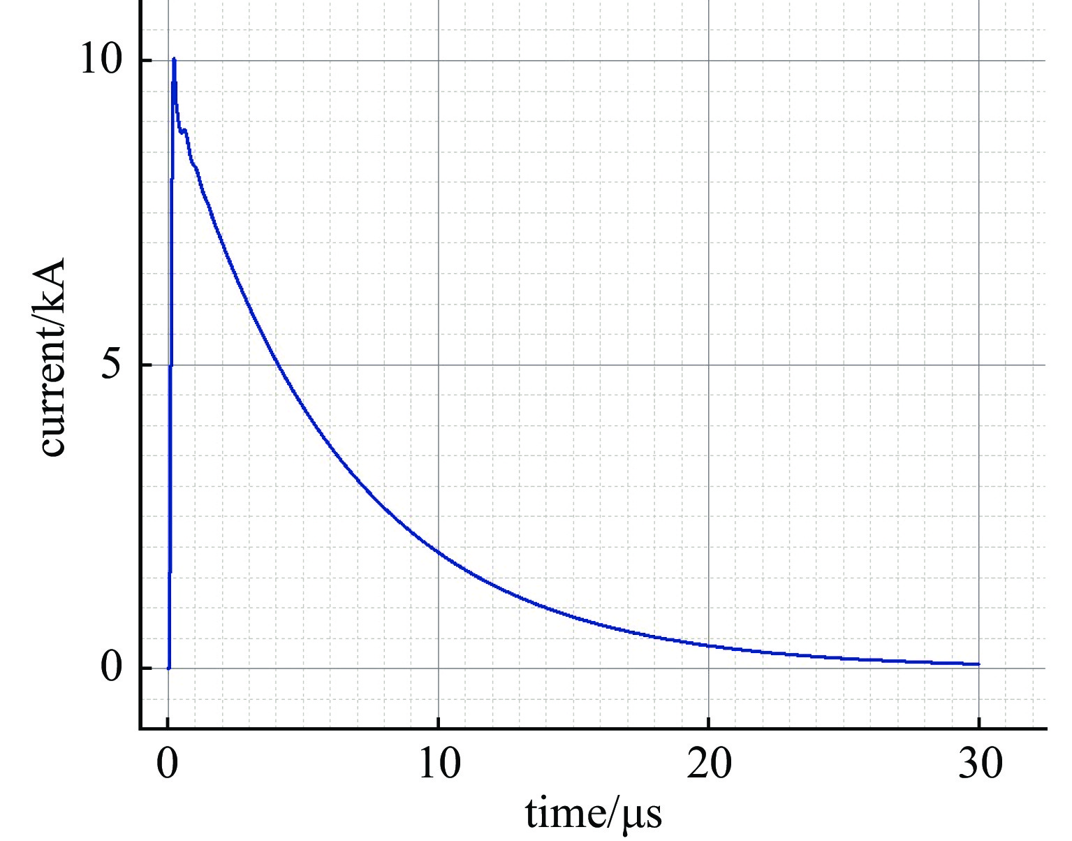
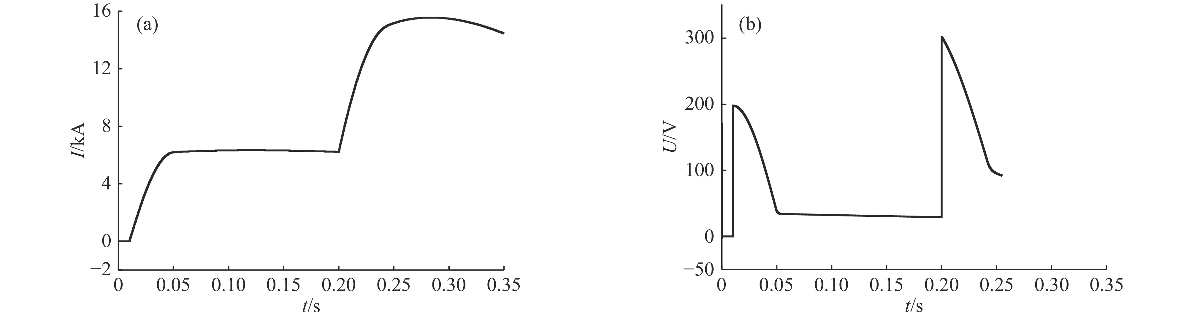
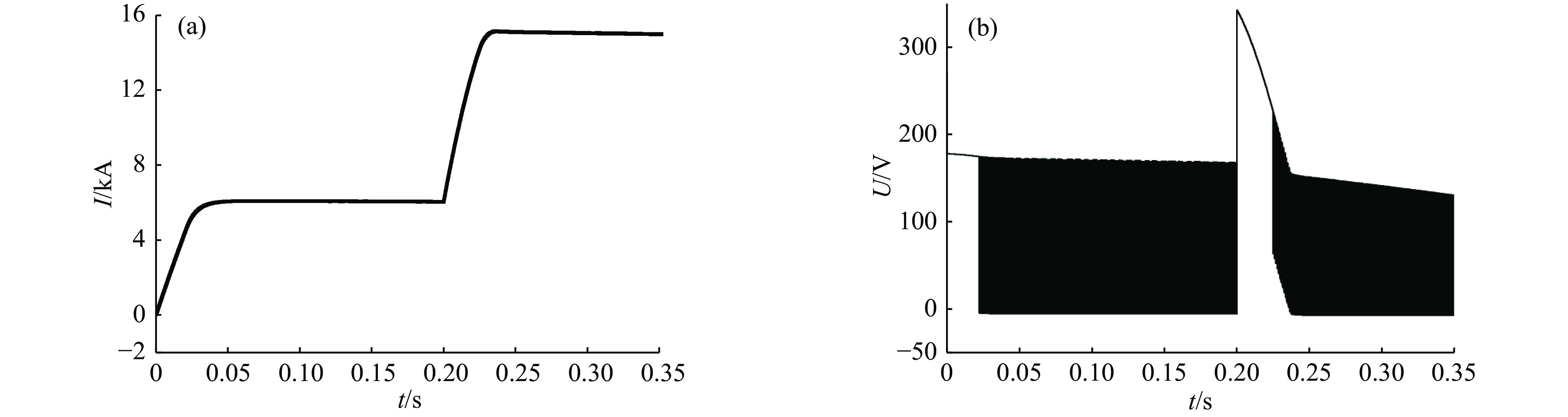
To meet the requirements of lightning electromagnetic pulse adaptability test of electronic and electrical equipment, it is necessary to develop a simulation device that meets the waveform of multiple pulse groups of lightning indirect effects. Multiple pulse groups with indirect lightning effects require the output of 60 adjustable interval current pulses, with a pulse current greater than 10 kA, a current front (10%−90%) of 100 ns, and a minimum current pulse time interval of only 50 μs. High requirements have been placed on analog devices. This article focuses on the simulation requirements of multiple pulse group currents for indirect effects of lightning, and has completed the design of a multiple pulse group simulation source for indirect effects of lightning. After the device is built, it can provide technical support for testing electronic and electrical equipment.
To meet the requirements of lightning electromagnetic pulse adaptability test of electronic and electrical equipment, it is necessary to develop a simulation device that meets the waveform of multiple pulse groups of lightning indirect effects. Multiple pulse groups with indirect lightning effects require the output of 60 adjustable interval current pulses, with a pulse current greater than 10 kA, a current front (10%−90%) of 100 ns, and a minimum current pulse time interval of only 50 μs. High requirements have been placed on analog devices. This article focuses on the simulation requirements of multiple pulse group currents for indirect effects of lightning, and has completed the design of a multiple pulse group simulation source for indirect effects of lightning. After the device is built, it can provide technical support for testing electronic and electrical equipment.


2024,
36: 025002.
doi: 10.11884/HPLPB202436.230211
Abstract:
The ability of electromagnetic emission mainly depends on the pulse power supply system, and the optimization of pulse power supply is one of the key technologies to make further breakthroughs in electromagnetic emission technology. Inductive energy storage type pulse power supply has great advantages in energy density and has far-reaching development potential. The XRAM pulse power supply based on series charging and parallel discharge has the advantages of simple structure and strong expandability. In this paper, the working principle of diode devices in multilevel XRAM power supply topology is analyzed, and a scheme is proposed to simplify the number of diode devices based on function classification. A simulation model is established for a 30-stage XRAM pulse power supply with a railgun load using ICCOS. Each power module consists of five stages, resulting in a total energy storage capacity of 365 kJ for the system, with an emission efficiency of nearly 20%. By comparing the simulation results of model performance indexes before and after simplification, it is proved that the simplified lower arm diode of the first stage is unfavorable to the operation of the multistage power supply. Simplifying the final countercurrent capacitor series diode in the multistage topology, and the antiparallel diode of charging thyristor under the premise of optimizing the countercurrent capacitor parameters, have no obvious effect on the discharge current of the power module.
The ability of electromagnetic emission mainly depends on the pulse power supply system, and the optimization of pulse power supply is one of the key technologies to make further breakthroughs in electromagnetic emission technology. Inductive energy storage type pulse power supply has great advantages in energy density and has far-reaching development potential. The XRAM pulse power supply based on series charging and parallel discharge has the advantages of simple structure and strong expandability. In this paper, the working principle of diode devices in multilevel XRAM power supply topology is analyzed, and a scheme is proposed to simplify the number of diode devices based on function classification. A simulation model is established for a 30-stage XRAM pulse power supply with a railgun load using ICCOS. Each power module consists of five stages, resulting in a total energy storage capacity of 365 kJ for the system, with an emission efficiency of nearly 20%. By comparing the simulation results of model performance indexes before and after simplification, it is proved that the simplified lower arm diode of the first stage is unfavorable to the operation of the multistage power supply. Simplifying the final countercurrent capacitor series diode in the multistage topology, and the antiparallel diode of charging thyristor under the premise of optimizing the countercurrent capacitor parameters, have no obvious effect on the discharge current of the power module.


2024,
36: 025003.
doi: 10.11884/HPLPB202436.230197
Abstract:
Nanosecond pulse electric field ablation requires the generation of thousands of volts of nanosecond pulses on a 100 Ω load, and accelerating the pulse front is beneficial for obtaining narrower nanosecond pulses. This article proposes a solid-state Marx generator with a fast front, which inserts an inductor into each stage of the circuit and allows the discharge tube and charging tube to conduct simultaneously for tens of nanoseconds. After the discharge tube is fully opened, the charging tube is turned off to discharge the load, eliminating the limitation of stray inductance on the pulse front by the discharge tube and discharge circuit, and obtaining a high-voltage pulse with a fast front. A 32 level Marx prototype was built, and in the experiment, a high-voltage pulse with a voltage rise of 35 ns, a pulse width of 800 ns, and a current of 186 A was obtained on a low resistance load of 100 Ω by adjusting the through time. We compared and analyzed the effect of the direct time between the charging tube and the discharge tube on the rising edge, and found that the longer the direct time, the faster the front of the pulse current. The maximum peak current at the output end can reach 186 A. This indicates that the pulse voltage source can effectively increase the current output and improve the system’s load capacity. Compared with traditional improvement methods, this scheme not only improves the system’s anti-interference ability, but also reduces the number of switches used and reduces the cost of pulse power supply.
Nanosecond pulse electric field ablation requires the generation of thousands of volts of nanosecond pulses on a 100 Ω load, and accelerating the pulse front is beneficial for obtaining narrower nanosecond pulses. This article proposes a solid-state Marx generator with a fast front, which inserts an inductor into each stage of the circuit and allows the discharge tube and charging tube to conduct simultaneously for tens of nanoseconds. After the discharge tube is fully opened, the charging tube is turned off to discharge the load, eliminating the limitation of stray inductance on the pulse front by the discharge tube and discharge circuit, and obtaining a high-voltage pulse with a fast front. A 32 level Marx prototype was built, and in the experiment, a high-voltage pulse with a voltage rise of 35 ns, a pulse width of 800 ns, and a current of 186 A was obtained on a low resistance load of 100 Ω by adjusting the through time. We compared and analyzed the effect of the direct time between the charging tube and the discharge tube on the rising edge, and found that the longer the direct time, the faster the front of the pulse current. The maximum peak current at the output end can reach 186 A. This indicates that the pulse voltage source can effectively increase the current output and improve the system’s load capacity. Compared with traditional improvement methods, this scheme not only improves the system’s anti-interference ability, but also reduces the number of switches used and reduces the cost of pulse power supply.


2024,
36: 025004.
doi: 10.11884/HPLPB202436.230287
Abstract:
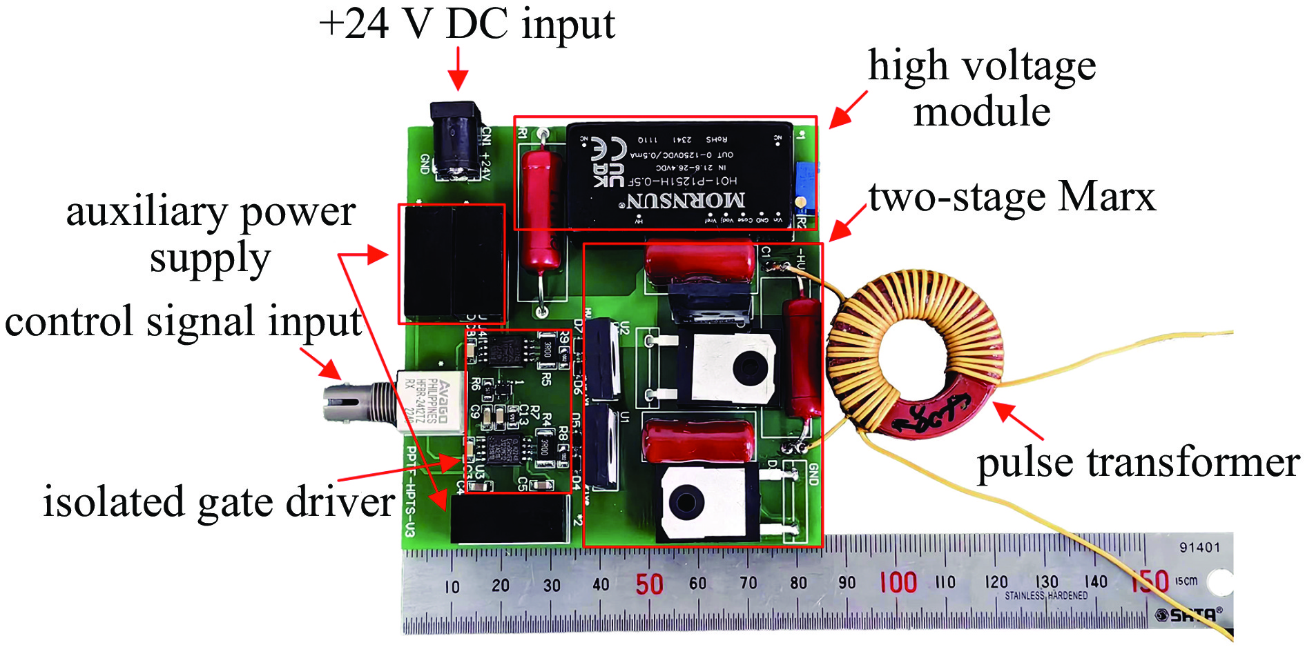
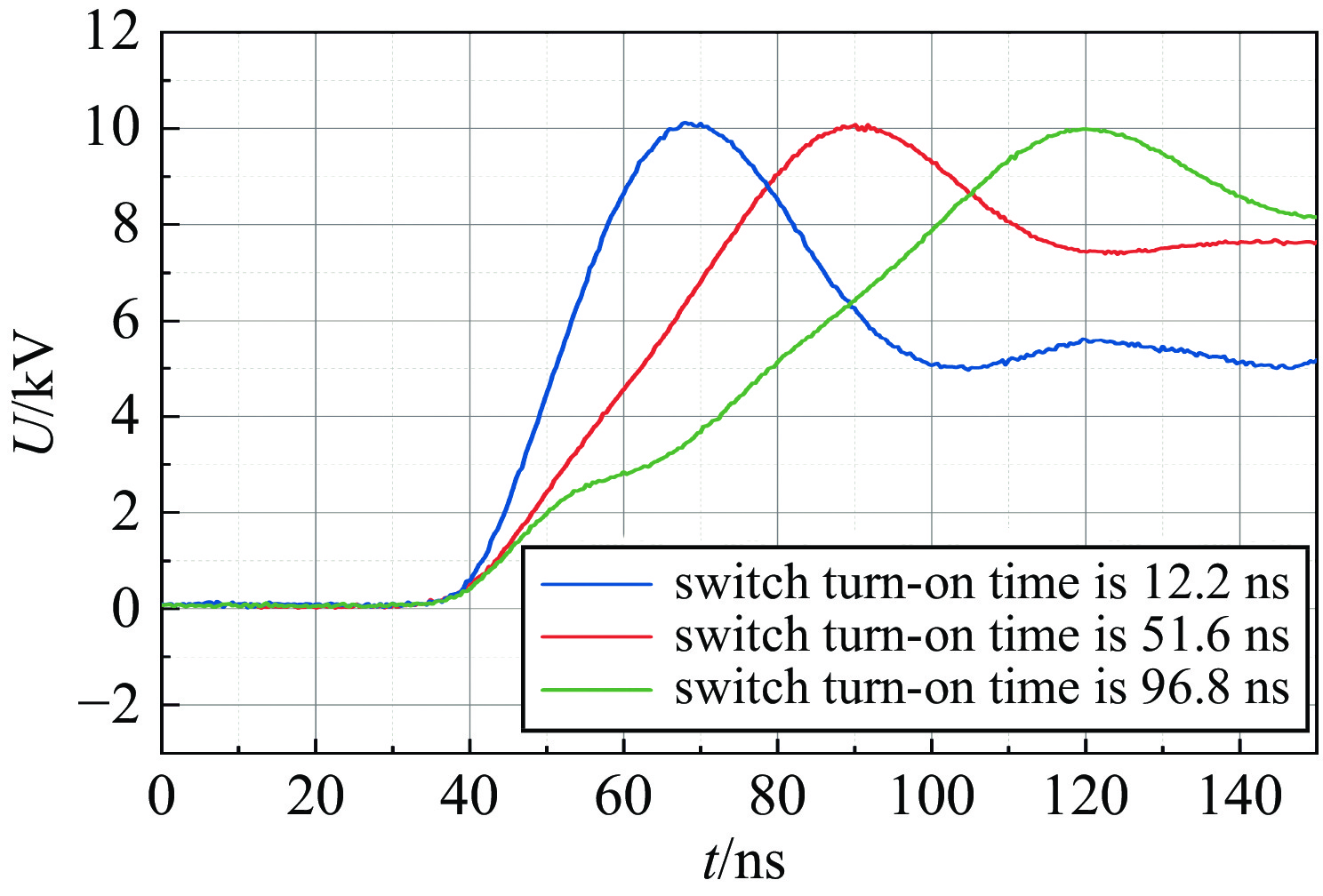
Using fast-rise-time high voltage pulse to trigger the switch is an important method to realize its low jitter operation. Combined with theoretical analysis, simulation results and experimental data, the main factors affecting the output pulse rise time of the pulse-transformer-based trigger source are investigated and a fast-rise-time solid-state trigger pulse generator is developed. Research results in this paper indicate that the key factors affecting the output pulse rise time are the leakage inductance of the pulse transformer, the turn-on speed of the semiconductor switch, and the pulse transformer turn ratio. A huge difference is observed in leakage inductance for different winding types. Among three winding types, the maximum leakage inductance is one order of magnitude greater than the minimum one. By selecting SiC MOSFET with a turn-on time less than 15 ns and using pulse transformer with low leakage inductance (<0.5 μH), a 20.4 ns (10%~90%) fast rise time and 16.5 kV output voltage can be achieved. By controlling the SiC MOSFET drive signal pulse width from 35−55 ns, the peak trigger current can vary from 35 to 55 A. The developed fast-rise-time solid-state trigger pulse generator can reliably trigger the vacuum surface flashover switch.
Using fast-rise-time high voltage pulse to trigger the switch is an important method to realize its low jitter operation. Combined with theoretical analysis, simulation results and experimental data, the main factors affecting the output pulse rise time of the pulse-transformer-based trigger source are investigated and a fast-rise-time solid-state trigger pulse generator is developed. Research results in this paper indicate that the key factors affecting the output pulse rise time are the leakage inductance of the pulse transformer, the turn-on speed of the semiconductor switch, and the pulse transformer turn ratio. A huge difference is observed in leakage inductance for different winding types. Among three winding types, the maximum leakage inductance is one order of magnitude greater than the minimum one. By selecting SiC MOSFET with a turn-on time less than 15 ns and using pulse transformer with low leakage inductance (<0.5 μH), a 20.4 ns (10%~90%) fast rise time and 16.5 kV output voltage can be achieved. By controlling the SiC MOSFET drive signal pulse width from 35−55 ns, the peak trigger current can vary from 35 to 55 A. The developed fast-rise-time solid-state trigger pulse generator can reliably trigger the vacuum surface flashover switch.


2024,
36: 025005.
doi: 10.11884/HPLPB202436.230329
Abstract:
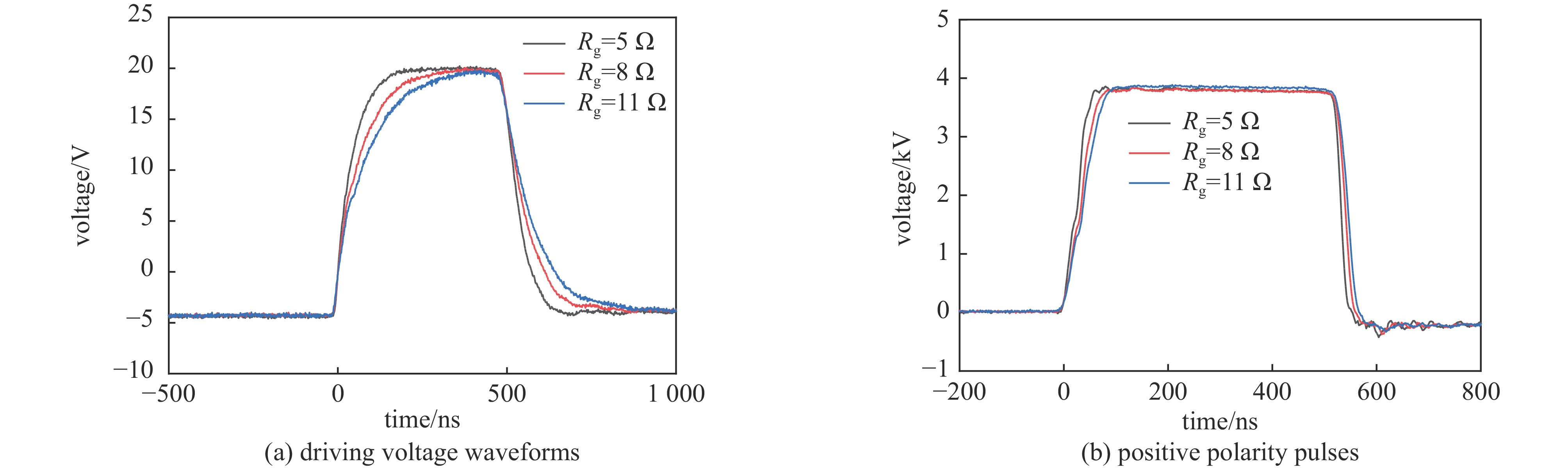
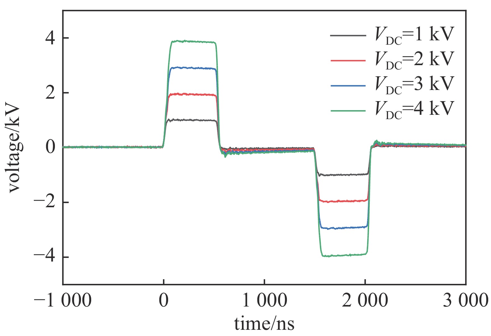
To meet the application requirements of pulsed electric field ablation and solve the problem of uneven distribution of unipolar pulse electric field, a bipolar submicrosecond high voltage pulse power supply with high repetition rate and nanosecond front based on the main circuit of half-bridge structure was developed. The pulse power supply is provided by the FPGA control signal, after amplifying the control signal by the driver chip, the photocoupler is used to drive multiple SiC MOSFETs. The drive circuit requires less components, its signal control timing is simple, and it can provide negative voltage bias, so that the switch tube is reliably turned off, which improves the anti-electromagnetic interference ability of the circuit, guranteeing stable operation of the power supply. Through resistance load experiment, the influence of different gate resistors on the driving voltage is compared and analyzed. The shorter the driving voltage rise time, the faster the bipolar high voltage pulse front is. The experimental results show that the designed high-frequency bipolar pulse power supply can stably generate repetitive bipolar nanosecond pulses on 100 Ω pure resistive load. The output voltage is adjustable from 0 to ±4 kV, the pulse width is adjustable from 0.2 μs to 1.0 μs, the phase delay between positive and negative pulses is adjustable from 0 to 1 ms, and the rising edge and falling edge are between 60 ns and 150 ns. The design structure of the bipolar pulse source circuit is compact, which can meet the application parameter requirements.
To meet the application requirements of pulsed electric field ablation and solve the problem of uneven distribution of unipolar pulse electric field, a bipolar submicrosecond high voltage pulse power supply with high repetition rate and nanosecond front based on the main circuit of half-bridge structure was developed. The pulse power supply is provided by the FPGA control signal, after amplifying the control signal by the driver chip, the photocoupler is used to drive multiple SiC MOSFETs. The drive circuit requires less components, its signal control timing is simple, and it can provide negative voltage bias, so that the switch tube is reliably turned off, which improves the anti-electromagnetic interference ability of the circuit, guranteeing stable operation of the power supply. Through resistance load experiment, the influence of different gate resistors on the driving voltage is compared and analyzed. The shorter the driving voltage rise time, the faster the bipolar high voltage pulse front is. The experimental results show that the designed high-frequency bipolar pulse power supply can stably generate repetitive bipolar nanosecond pulses on 100 Ω pure resistive load. The output voltage is adjustable from 0 to ±4 kV, the pulse width is adjustable from 0.2 μs to 1.0 μs, the phase delay between positive and negative pulses is adjustable from 0 to 1 ms, and the rising edge and falling edge are between 60 ns and 150 ns. The design structure of the bipolar pulse source circuit is compact, which can meet the application parameter requirements.


2024,
36: 025006.
doi: 10.11884/HPLPB202436.230148
Abstract:
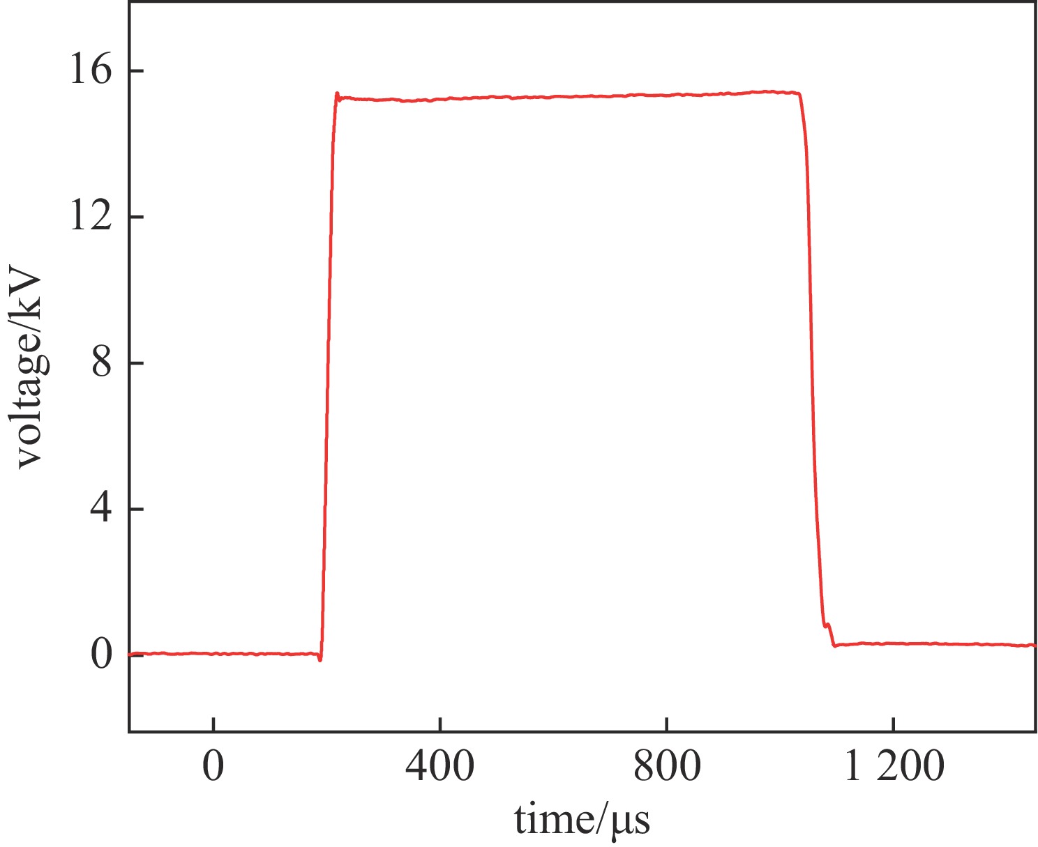
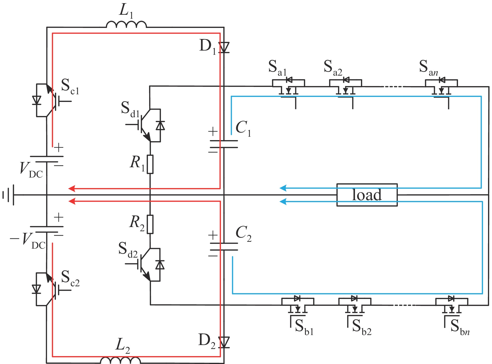
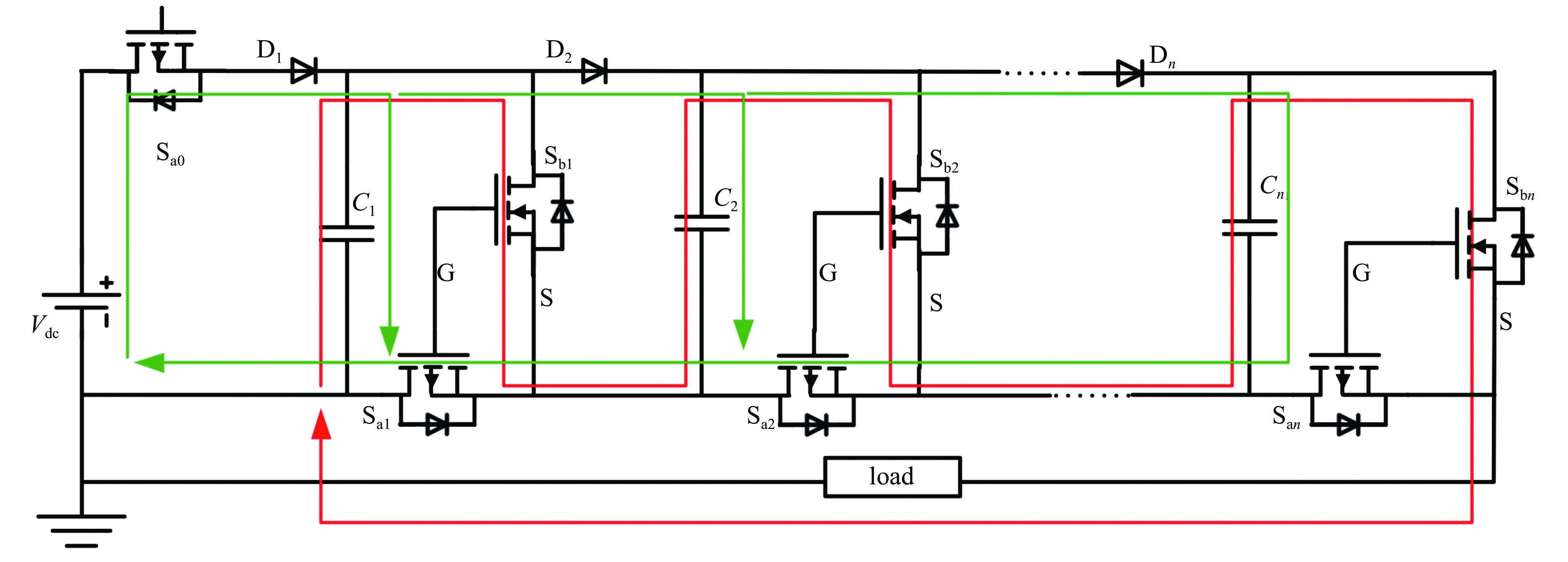
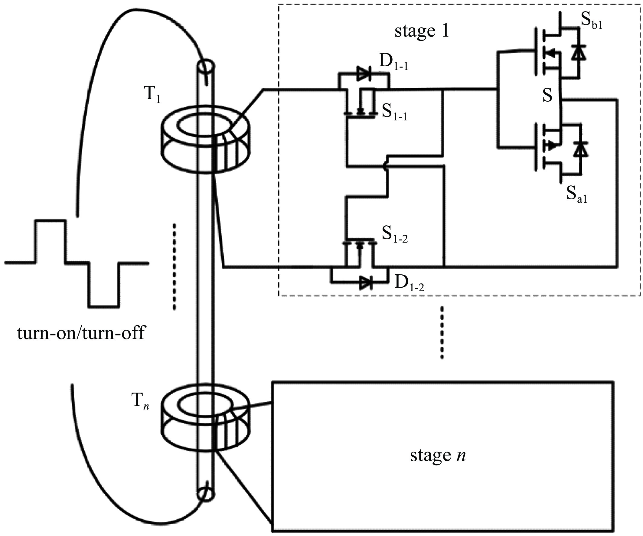
This paper proposes compact solid-state Marx generator based on half-bridge structure. In each stage, an NPN MOSFET as the charging switch and a PNP MOSFET as the discharging switch forms a half-bridge circuit, and both their gates and sources are short circuited so that they can be triggered with the same signal. Using many transformers with their primary windings in series, only one half-bridge circuit on the primary side is used to transfer both the driving power and control signals. Then all the charging switches and discharging switches are driven simultaneously, which greatly simplifies the structure and size of solid-state Marx generators and reduces costs. In this way, a 24-stage solid-state Marx generator prototype was built, and high-voltage square pulses of 10 kV, 1 kHz and 5 μs was obtained on a 10 kΩ resistive load. The feasibility of the scheme is verified, and the size of the main circuit is only 20 cm (length)×13 cm (width)×5.5 cm (height).
This paper proposes compact solid-state Marx generator based on half-bridge structure. In each stage, an NPN MOSFET as the charging switch and a PNP MOSFET as the discharging switch forms a half-bridge circuit, and both their gates and sources are short circuited so that they can be triggered with the same signal. Using many transformers with their primary windings in series, only one half-bridge circuit on the primary side is used to transfer both the driving power and control signals. Then all the charging switches and discharging switches are driven simultaneously, which greatly simplifies the structure and size of solid-state Marx generators and reduces costs. In this way, a 24-stage solid-state Marx generator prototype was built, and high-voltage square pulses of 10 kV, 1 kHz and 5 μs was obtained on a 10 kΩ resistive load. The feasibility of the scheme is verified, and the size of the main circuit is only 20 cm (length)×13 cm (width)×5.5 cm (height).


2024,
36: 025007.
doi: 10.11884/HPLPB202436.230322
Abstract:
Modular multilevel converter (MMC) has become an effective solution for new all-solid-state special high-voltage power supply, and its lightweight design to save equipment space cost has become a research hotspot. The primary factor limiting power density in MMC is the large size capacitance of submodule (SM), and to reduce the demand for the capacitance of the sub-module in modular multilevel converter, and increase system power density, an improved MMC(I-MMC) topology is proposed. Using isolated switched capacitor converters, a pair of SMs of the upper and lower arms are interconnected through a high frequency link. In the research, synchronous control was adopted on both sides of the high-frequency chain connecting the pair of SMs in the phase unit to make the SM capacitors present the characteristics of switched capacitors, realize free transfer of fluctuating power between the capacitors, and eliminate the fluctuation components of the oppostite phased fundamental frequency and triple frequency. Combining MMC operation modulation ratio and power factor, we analyzed the value of the SM capacitor after the fundamental frequency and triple frequency fluctuation components had been eliminated, and completed the modular design. This solution can reduce the sub-module capacitance to 1/4 of the conventional MMC's capacitance. Simulation and experimental results verify the correctness and the validity of the proposed topology scheme.
Modular multilevel converter (MMC) has become an effective solution for new all-solid-state special high-voltage power supply, and its lightweight design to save equipment space cost has become a research hotspot. The primary factor limiting power density in MMC is the large size capacitance of submodule (SM), and to reduce the demand for the capacitance of the sub-module in modular multilevel converter, and increase system power density, an improved MMC(I-MMC) topology is proposed. Using isolated switched capacitor converters, a pair of SMs of the upper and lower arms are interconnected through a high frequency link. In the research, synchronous control was adopted on both sides of the high-frequency chain connecting the pair of SMs in the phase unit to make the SM capacitors present the characteristics of switched capacitors, realize free transfer of fluctuating power between the capacitors, and eliminate the fluctuation components of the oppostite phased fundamental frequency and triple frequency. Combining MMC operation modulation ratio and power factor, we analyzed the value of the SM capacitor after the fundamental frequency and triple frequency fluctuation components had been eliminated, and completed the modular design. This solution can reduce the sub-module capacitance to 1/4 of the conventional MMC's capacitance. Simulation and experimental results verify the correctness and the validity of the proposed topology scheme.


2024,
36: 025008.
doi: 10.11884/HPLPB202436.230173
Abstract:
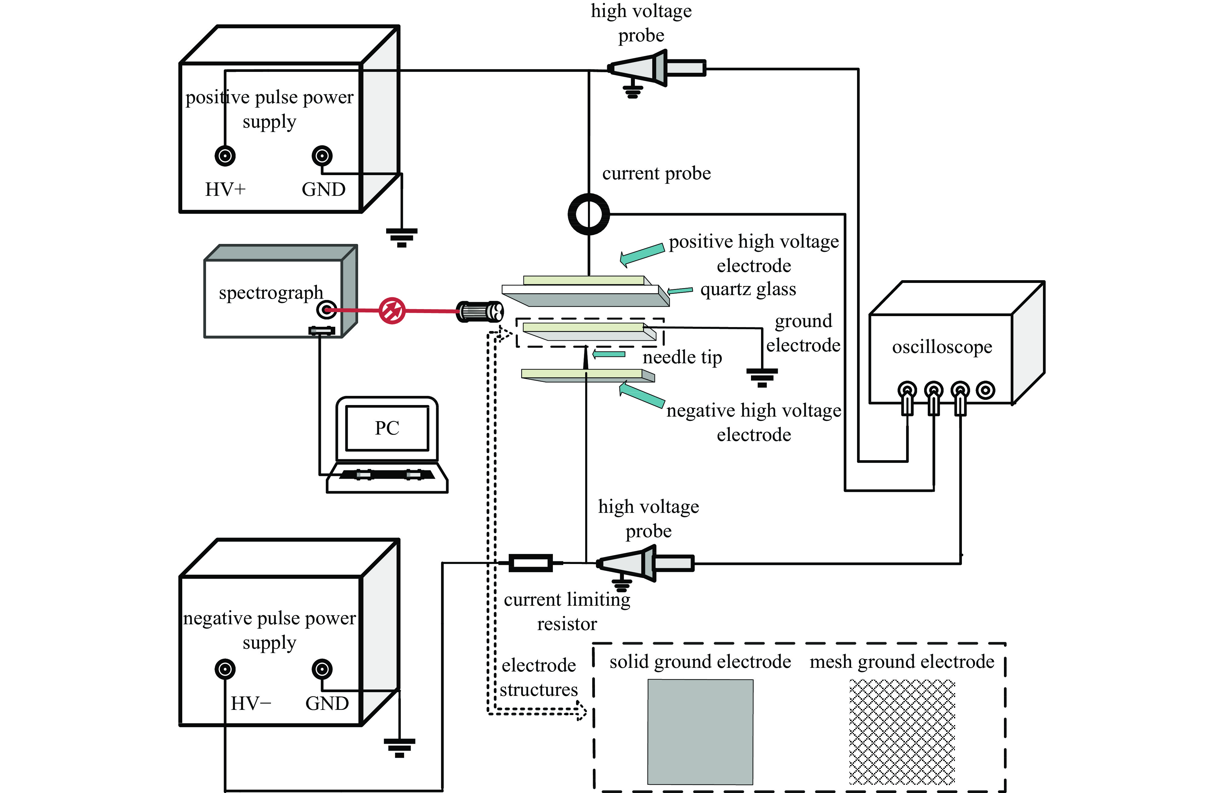
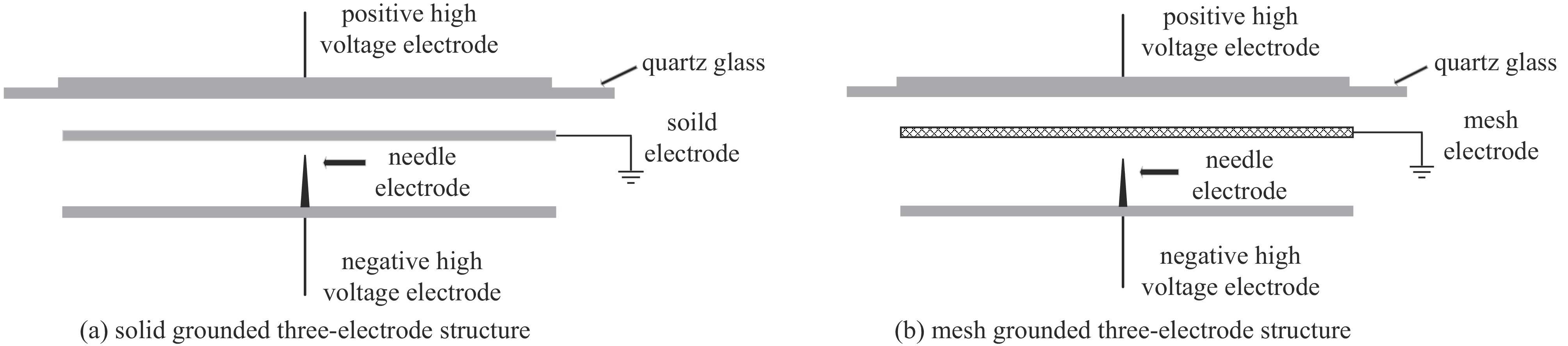
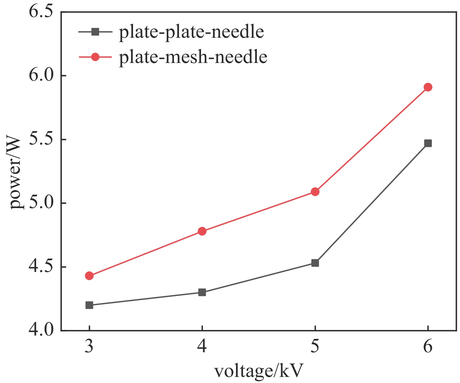
Dielectric barrier discharge (DBD) is widely used in industry, but the efficiency limits its further application. This paper proposes a three-electrode structure combining a DBD structure and a needle-plate structure. A positive polarity pulsed power supply is applied to the DBD electrode and a negative polarity pulsed power supply is applied to the needle plate electrode. The discharge characteristics, phenomena and spectral intensity of the three-electrode DBD under different structures are analyzed. The results show that the three-electrode structure is more beneficial to the generation of DBD discharge channels, and its discharge uniformity and luminous intensity are stronger than that of the two-electrode DBD, especially under the condition of mesh grounded electrode. When the positive polarity voltage of the three-electrode structure was maintained at 11 kV and the negative polarity voltage was −5 kV, the peak discharge current of DBD in the mesh grounded three-electrode reached 1.54 A, while the peak discharge currents of DBD in the solid grounded three-electrode and the traditional two-electrode were 1.14 A and 0.74 A respectively. During the period of the negative polarity pulse maintenance, the needle mesh gap was in the state of breakdown, and the DBD discharges appeared to have a large discharge current. In the three-electrode structure, the three-electrode DBD discharges also become more intense with the increase of the negative polarity voltage applied to the needle plate. According to the discharge spectra of DBD under different structures, spectral intensity of excited particles is the strongest among the three-electrode DBD grounded with wire mesh. This trend is consistent with the discharge current and power of DBD.
Dielectric barrier discharge (DBD) is widely used in industry, but the efficiency limits its further application. This paper proposes a three-electrode structure combining a DBD structure and a needle-plate structure. A positive polarity pulsed power supply is applied to the DBD electrode and a negative polarity pulsed power supply is applied to the needle plate electrode. The discharge characteristics, phenomena and spectral intensity of the three-electrode DBD under different structures are analyzed. The results show that the three-electrode structure is more beneficial to the generation of DBD discharge channels, and its discharge uniformity and luminous intensity are stronger than that of the two-electrode DBD, especially under the condition of mesh grounded electrode. When the positive polarity voltage of the three-electrode structure was maintained at 11 kV and the negative polarity voltage was −5 kV, the peak discharge current of DBD in the mesh grounded three-electrode reached 1.54 A, while the peak discharge currents of DBD in the solid grounded three-electrode and the traditional two-electrode were 1.14 A and 0.74 A respectively. During the period of the negative polarity pulse maintenance, the needle mesh gap was in the state of breakdown, and the DBD discharges appeared to have a large discharge current. In the three-electrode structure, the three-electrode DBD discharges also become more intense with the increase of the negative polarity voltage applied to the needle plate. According to the discharge spectra of DBD under different structures, spectral intensity of excited particles is the strongest among the three-electrode DBD grounded with wire mesh. This trend is consistent with the discharge current and power of DBD.


2024,
36: 025009.
doi: 10.11884/HPLPB202436.230158
Abstract:
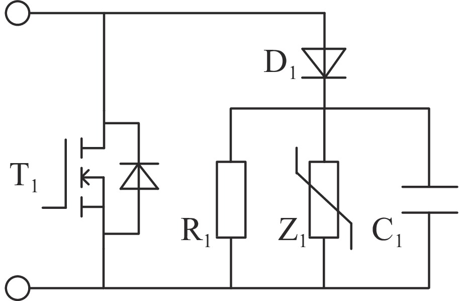
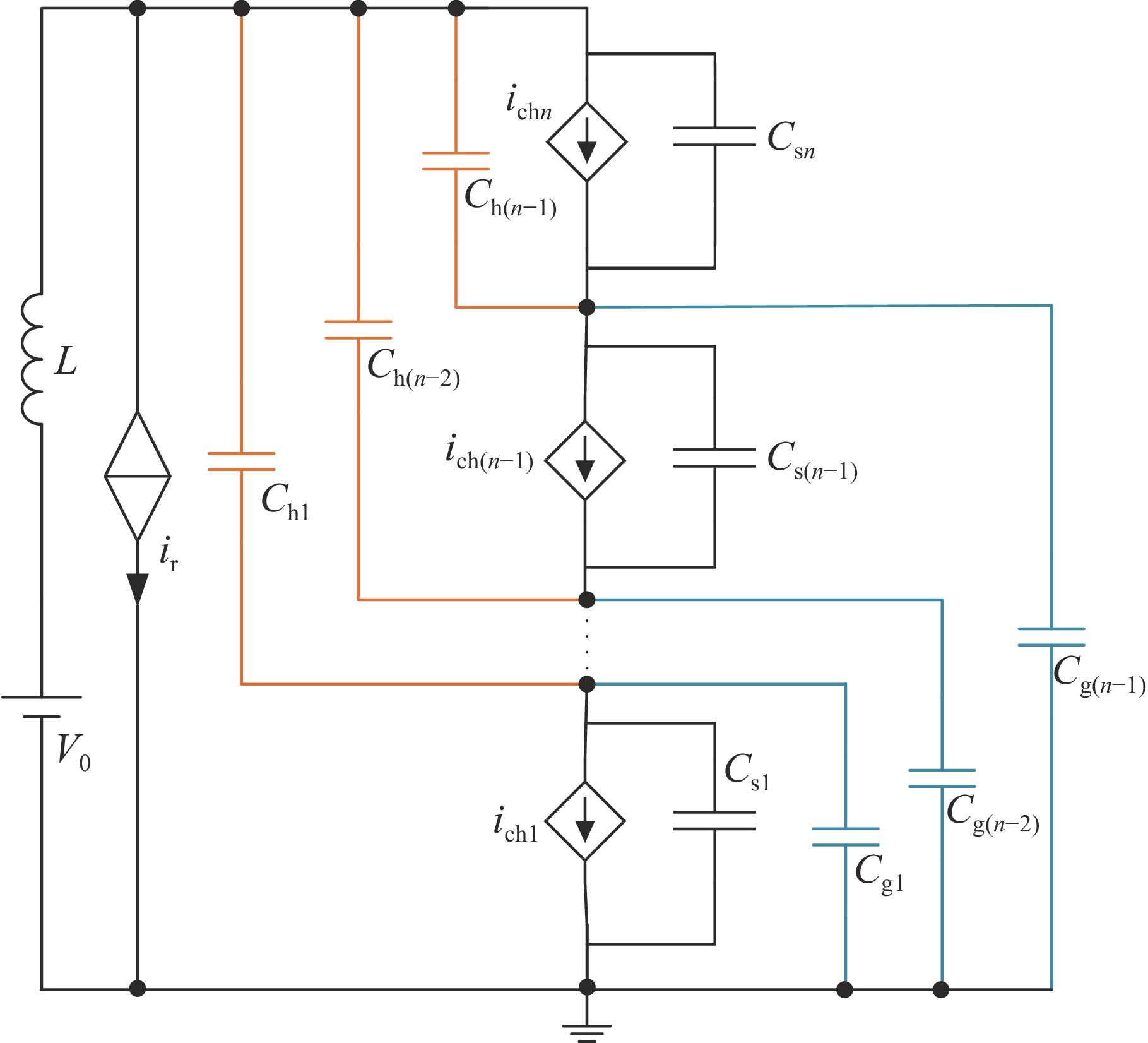
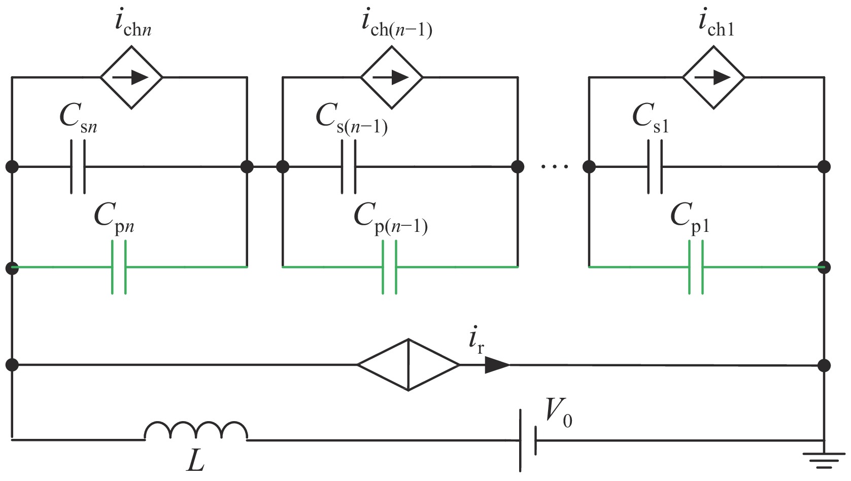
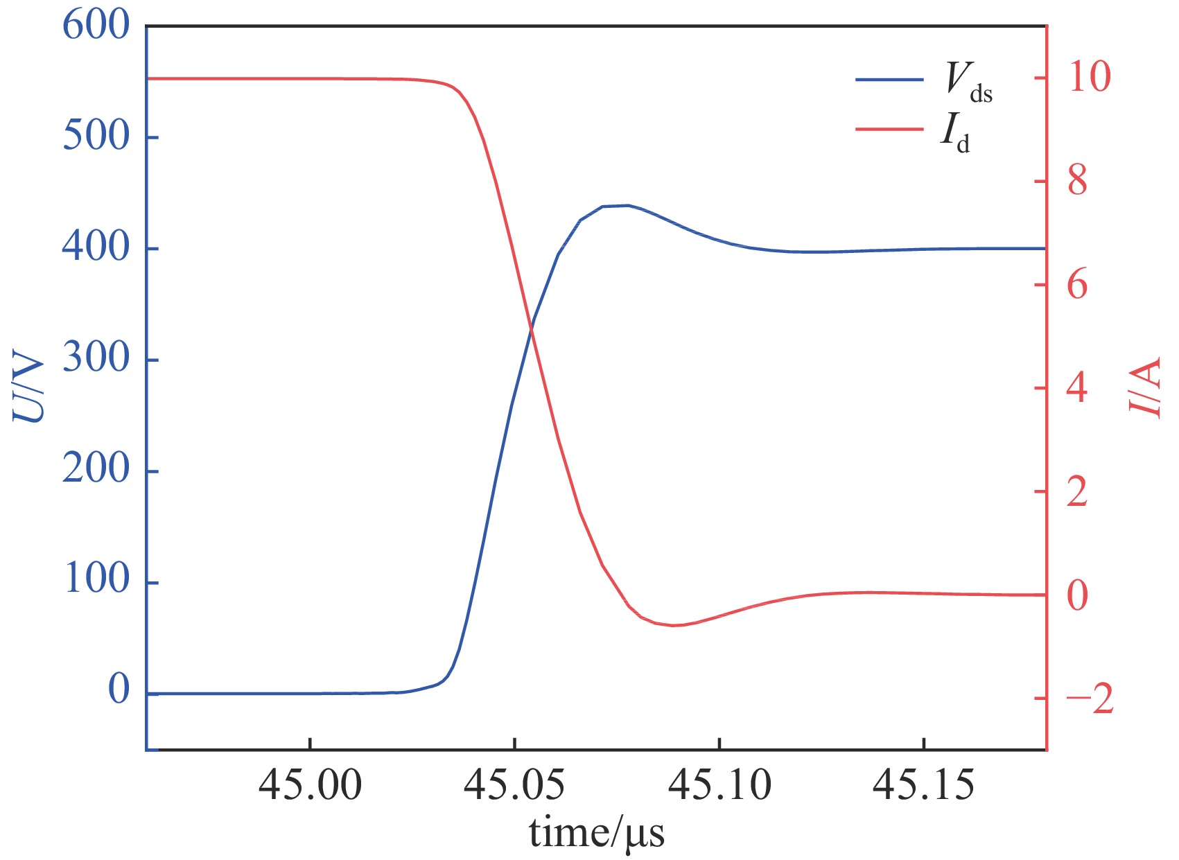
The ion source and electron gyrotron of the fusion auxiliary heating system are prone to failure and expensive. To protect them, it is necessary to study the high voltage switch scheme. The parameter design methods of high voltage protection switch snubber circuit are lack of relevant theoretical design methods currently, and the snubber circuit schemes are isoparametric design schemes because the influence of distributed capacitance is not taken into account in the design process. The voltage-balancing effect of this method is not ideal. To solve the problems existing in the current parameter design, we have established the MOSFET model with snubber circuit and stray inductor and analyze its turn-off process, thus to obtain the theoretical design method and expression of snubber circuit for suppressing voltage spike. Taking the distributed capacitance into consideration in series voltage-balancing and constructing the isoelectric point, we have established and analyzed the equivalent circuit, and obtained the non-equal parameter design method and expression of snubber circuit according to the charge equation. This parameter design method can compensate the uneven voltage distribution caused by distributed capacitance and guide the voltage-balancing scheme design of high voltage protection switch better. To verify the rationality of the parameter design, we have a carried out, simulation analysis. which shows that the overall design scheme can meet the design requirements of peak suppression and voltage-balancing.
The ion source and electron gyrotron of the fusion auxiliary heating system are prone to failure and expensive. To protect them, it is necessary to study the high voltage switch scheme. The parameter design methods of high voltage protection switch snubber circuit are lack of relevant theoretical design methods currently, and the snubber circuit schemes are isoparametric design schemes because the influence of distributed capacitance is not taken into account in the design process. The voltage-balancing effect of this method is not ideal. To solve the problems existing in the current parameter design, we have established the MOSFET model with snubber circuit and stray inductor and analyze its turn-off process, thus to obtain the theoretical design method and expression of snubber circuit for suppressing voltage spike. Taking the distributed capacitance into consideration in series voltage-balancing and constructing the isoelectric point, we have established and analyzed the equivalent circuit, and obtained the non-equal parameter design method and expression of snubber circuit according to the charge equation. This parameter design method can compensate the uneven voltage distribution caused by distributed capacitance and guide the voltage-balancing scheme design of high voltage protection switch better. To verify the rationality of the parameter design, we have a carried out, simulation analysis. which shows that the overall design scheme can meet the design requirements of peak suppression and voltage-balancing.


2024,
36: 025010.
doi: 10.11884/HPLPB202436.230207
Abstract:
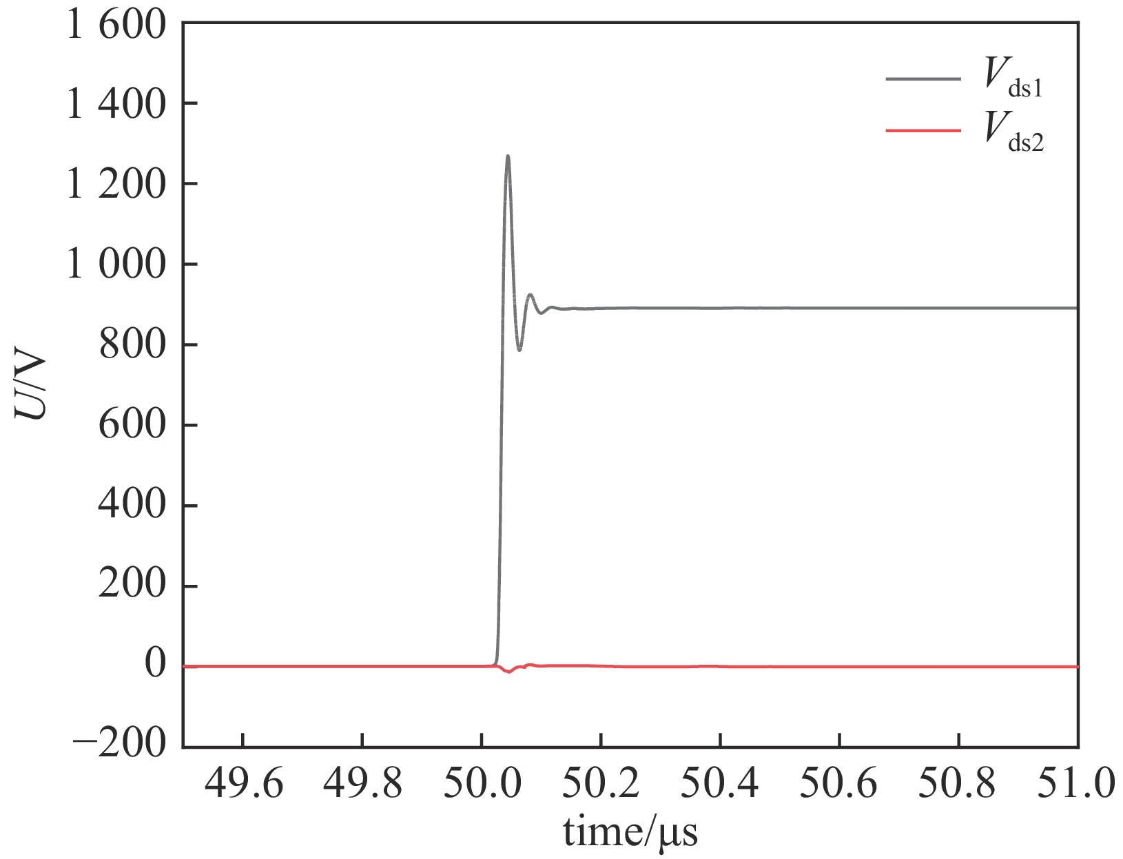
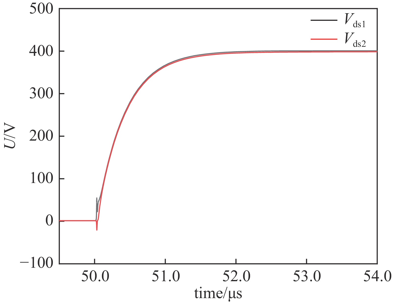
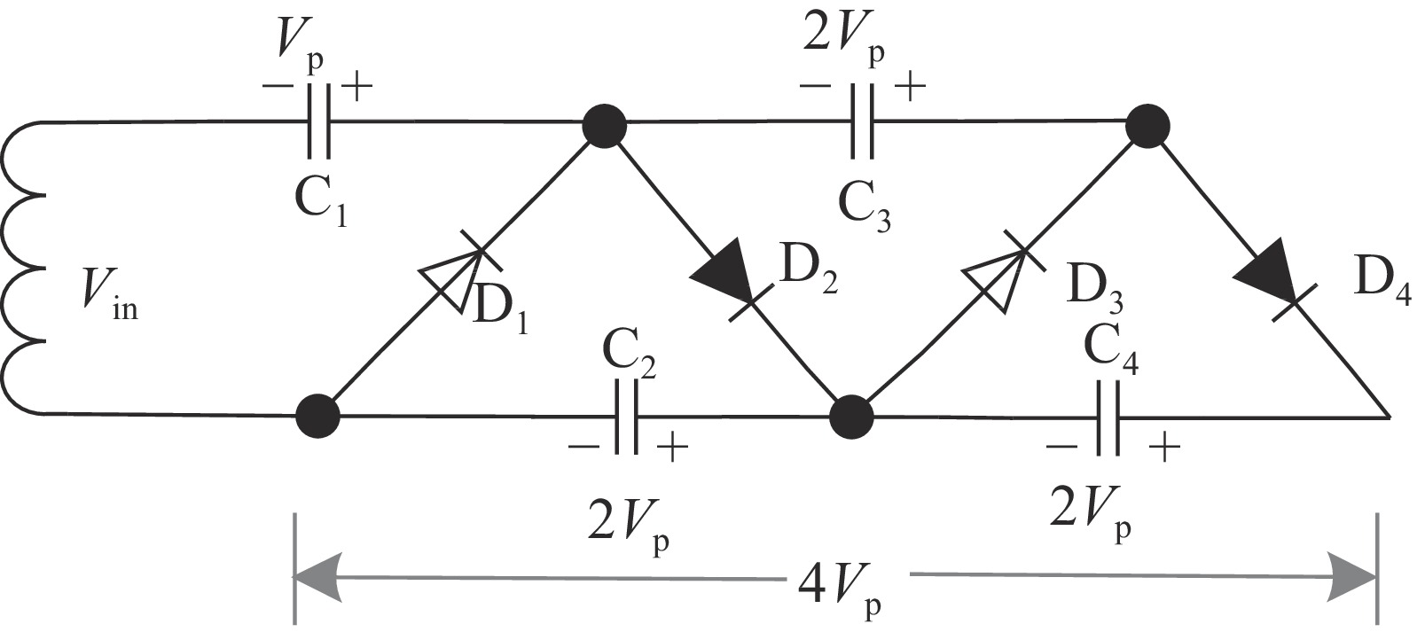
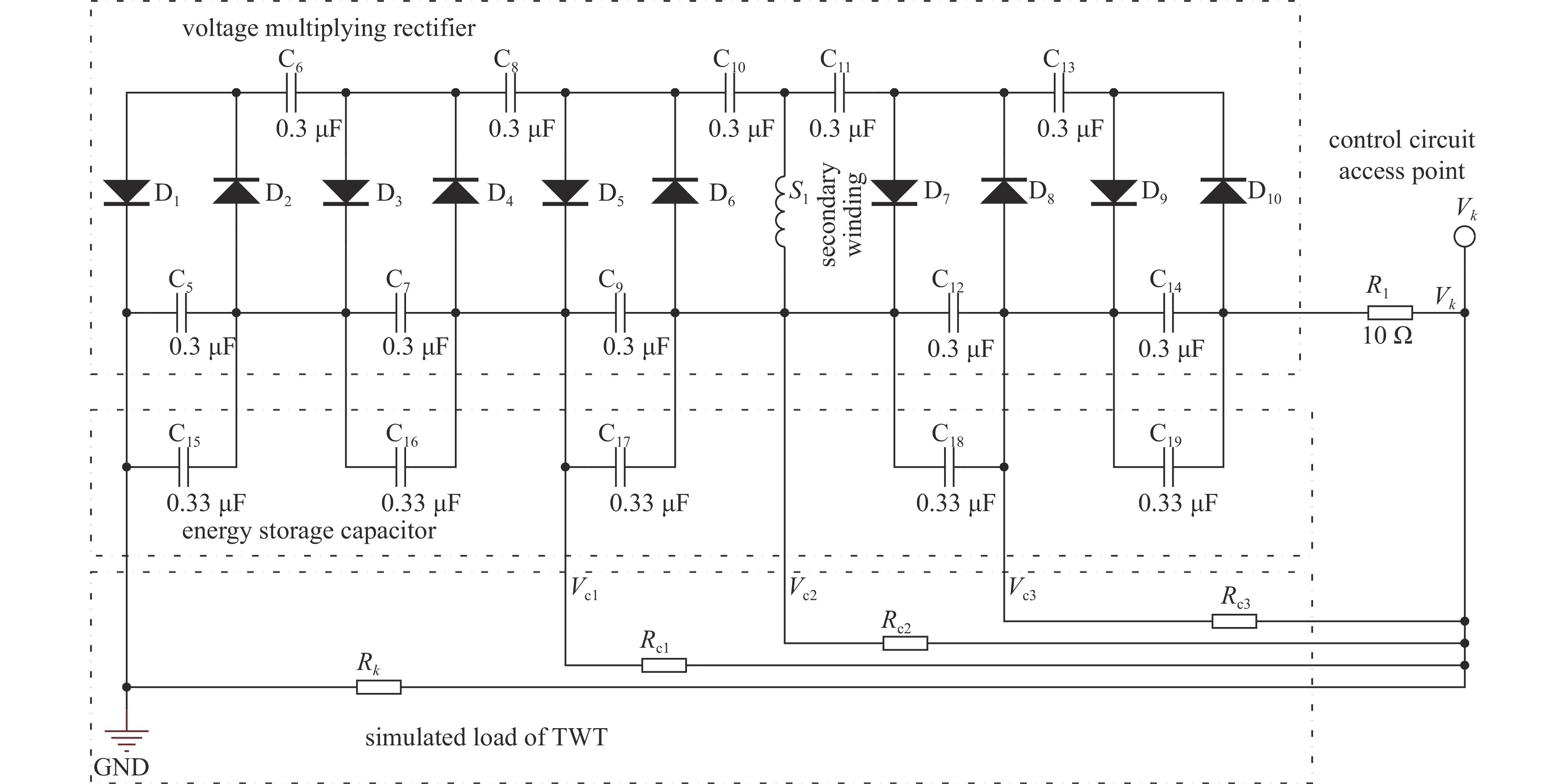
To meet the demand of radar for miniaturization of transmitter, a miniaturized high-voltage power supply is designed for a certain type of TWT. The high voltage power supply adopts a phase shifted full bridge topology structure, and the high voltage rectifier circuit uses SiC diodes to improve the power density of the power supply. The miniaturized pulse high-voltage power supply has been developed, with a cathode voltage of −6.5 kV, a maximum working pulse width of 2 ms, and a peak power of 1600 W. The joint test with traveling-wave tube shows that the output RF power of TWT is stable during pulse operation. The test results verify the feasibility of the design method.
To meet the demand of radar for miniaturization of transmitter, a miniaturized high-voltage power supply is designed for a certain type of TWT. The high voltage power supply adopts a phase shifted full bridge topology structure, and the high voltage rectifier circuit uses SiC diodes to improve the power density of the power supply. The miniaturized pulse high-voltage power supply has been developed, with a cathode voltage of −6.5 kV, a maximum working pulse width of 2 ms, and a peak power of 1600 W. The joint test with traveling-wave tube shows that the output RF power of TWT is stable during pulse operation. The test results verify the feasibility of the design method.


2024,
36: 025011.
doi: 10.11884/HPLPB202436.230159
Abstract:
Negative-ion based neutral beam injection is an indispensable auxiliary heating method for future large tokamak devices. The acceleration grid power supply in the neutral beam system requires an output voltage of -200 kV and a power of 5 MW, and often faces special conditions of sudden short-circuit and disconnection of the load. The design of the high-voltage components is still missing in the research of the acceleration grid power supply. The insulation design of the high-voltage components is a critical part of the power supply development process. In this paper, the circuit parameters of the step-up transformer, high-voltage rectifier and high-voltage filter of the high-voltage part of the power supply are calculated according to the power supply index and the characteristics of the special working conditions, the engineering design based on oil-immersed insulation of these parts is also carried out, and the insulation is verified by finite element simulation analysis. The simulation results show that the maximum electric field strength in these components is 16.22 kV/mm, which is less than the transformer oil breakdown field strength and has 2 times the insulation margin. The structural design of the high-voltage components in this paper can meet the insulation requirements of the power supply.
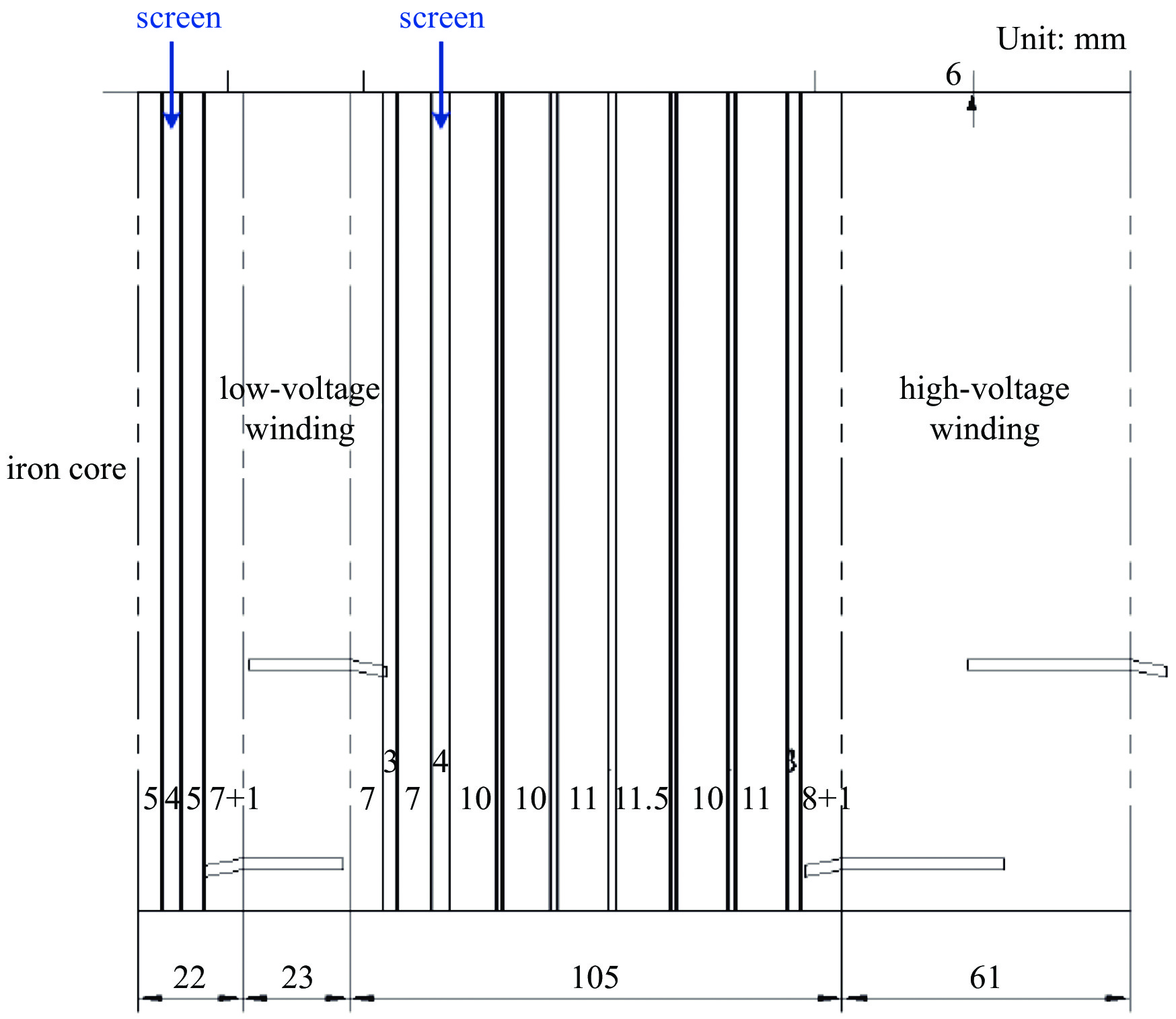
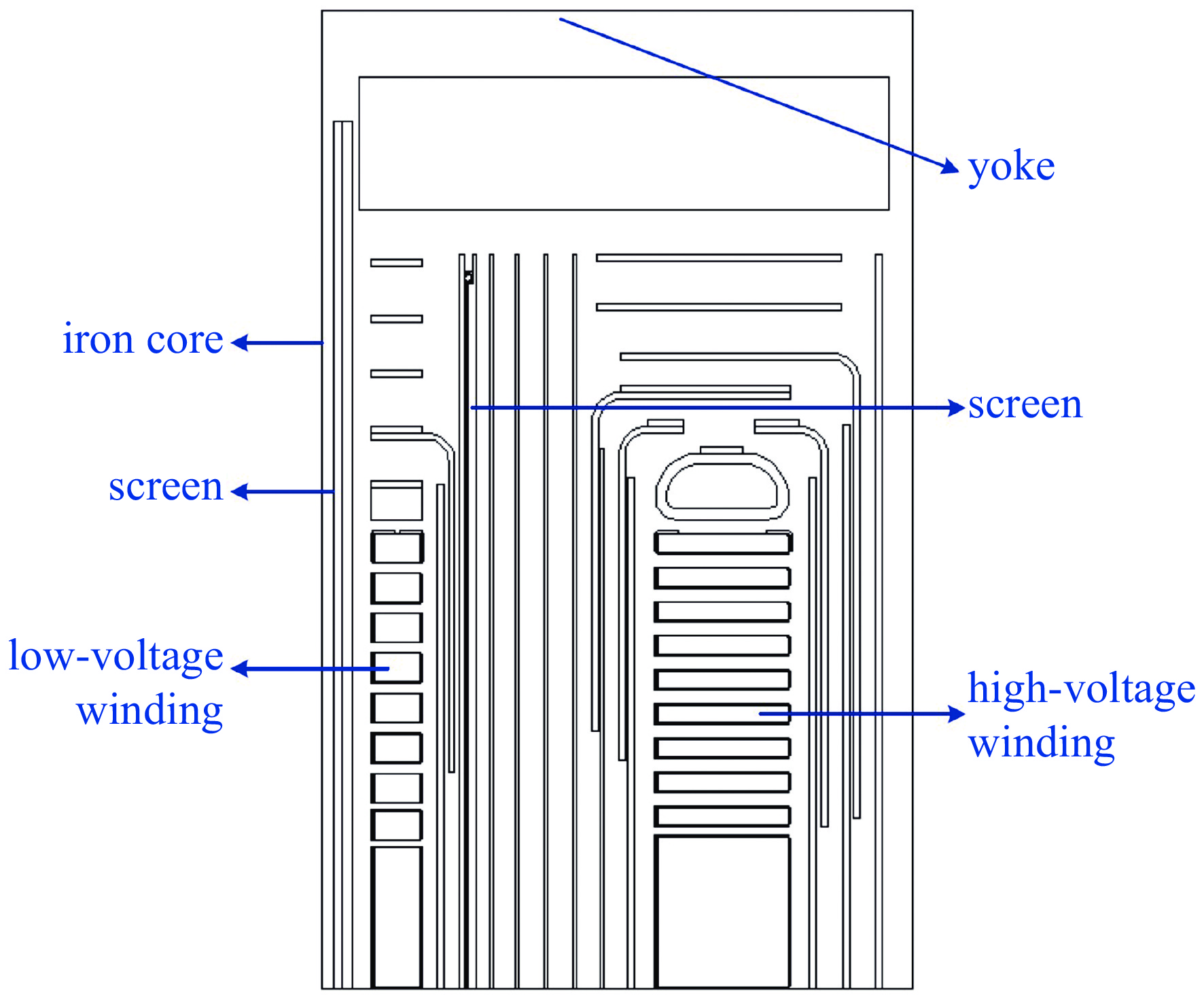
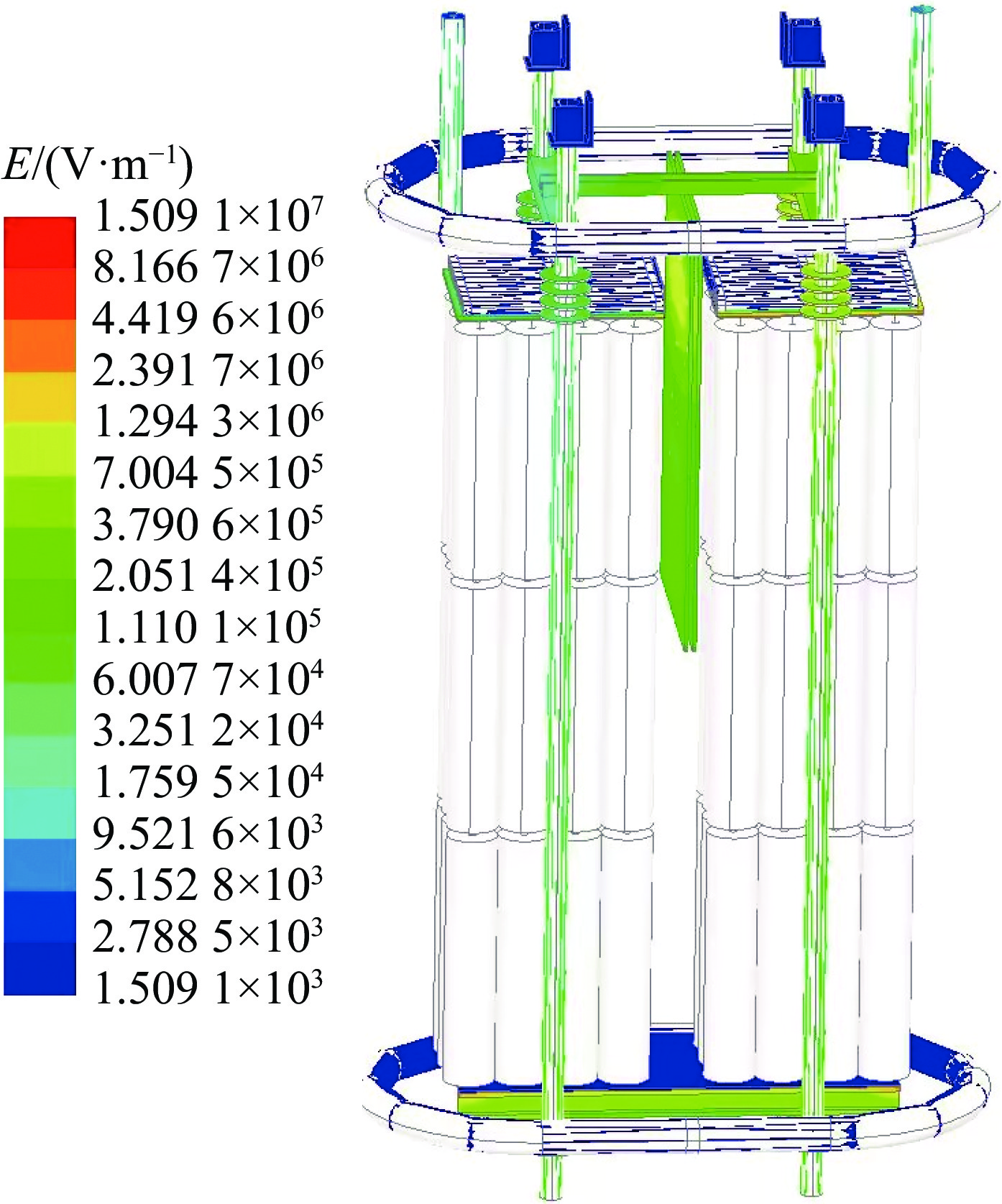
Negative-ion based neutral beam injection is an indispensable auxiliary heating method for future large tokamak devices. The acceleration grid power supply in the neutral beam system requires an output voltage of -200 kV and a power of 5 MW, and often faces special conditions of sudden short-circuit and disconnection of the load. The design of the high-voltage components is still missing in the research of the acceleration grid power supply. The insulation design of the high-voltage components is a critical part of the power supply development process. In this paper, the circuit parameters of the step-up transformer, high-voltage rectifier and high-voltage filter of the high-voltage part of the power supply are calculated according to the power supply index and the characteristics of the special working conditions, the engineering design based on oil-immersed insulation of these parts is also carried out, and the insulation is verified by finite element simulation analysis. The simulation results show that the maximum electric field strength in these components is 16.22 kV/mm, which is less than the transformer oil breakdown field strength and has 2 times the insulation margin. The structural design of the high-voltage components in this paper can meet the insulation requirements of the power supply.


2024,
36: 025012.
doi: 10.11884/HPLPB202436.230243
Abstract:
Toroidal magnetic field should match frequency of the electron cyclotron wave in pre-ionization process of the Tokamak device. The existing electron cyclotron wave frequency of the NCST (Nanchang Spherical Tokamak) is low. A new toroidal coil current generation scheme is proposed to match the current electron cyclotron wave frequency. A low current step is added before the existing flat top current of original scheme. After reviewing the original scheme of the toroidal coil power supply of NCST, two schemes of full control and semi-control are designed. Advantages and disadvantages of the two schemes are compared from four aspects: high order harmonics of voltage and current, controllability and ripple of current, modification cost and installation convenience, and finally the semi-control transformation scheme is selected. The power supply cabinet is modified according to the field conditions with minimum alteration. Actual test results show that the two current steps are connected normally, and the width and amplitude of low current steps are adjustable, which meets the transformation requirements.
Toroidal magnetic field should match frequency of the electron cyclotron wave in pre-ionization process of the Tokamak device. The existing electron cyclotron wave frequency of the NCST (Nanchang Spherical Tokamak) is low. A new toroidal coil current generation scheme is proposed to match the current electron cyclotron wave frequency. A low current step is added before the existing flat top current of original scheme. After reviewing the original scheme of the toroidal coil power supply of NCST, two schemes of full control and semi-control are designed. Advantages and disadvantages of the two schemes are compared from four aspects: high order harmonics of voltage and current, controllability and ripple of current, modification cost and installation convenience, and finally the semi-control transformation scheme is selected. The power supply cabinet is modified according to the field conditions with minimum alteration. Actual test results show that the two current steps are connected normally, and the width and amplitude of low current steps are adjustable, which meets the transformation requirements.


2024,
36: 025013.
doi: 10.11884/HPLPB202436.230151
Abstract:
This paper proposes, a two-stage variable bus voltage high-voltage capacitor charging power supply technical scheme which adds a one-stage totem-pole bridgeless power factor correction (PFC) circuit on the basis of the half-bridge LLC resonant circuit, and solves the problem of the decline in charging efficiency caused by the excessive operating frequency variation range of the traditional LLC resonant power supply when the output voltage is higher. Since the totem-pole circuit itself has the function of power factor correction, the power supply design also has the advantage of being able to draw power directly from the grid without affecting the power quality of the grid. This paper first introduces the circuit topology and working principle of the two parts of this power supply design, and analyzes the output characteristics of the power supply under capacitive load by the equivalent resistance method. For the pre-stage totem-pole circuit, a double-loop controller is designed to realize the control of bus voltage and power factors, and a constant current controller with proportional-integral (PI) plus low-pass filtering control is proposed for the post-stage LLC circuit to reduce the adverse effects of high-frequency noise. Finally, through model construction and simulation analysis, the charging characteristics of high-voltage capacitor charging power supply at 3000V/1 A are studied, and the feasibility of the technical scheme, design and control strategy of the power supply is verified.
This paper proposes, a two-stage variable bus voltage high-voltage capacitor charging power supply technical scheme which adds a one-stage totem-pole bridgeless power factor correction (PFC) circuit on the basis of the half-bridge LLC resonant circuit, and solves the problem of the decline in charging efficiency caused by the excessive operating frequency variation range of the traditional LLC resonant power supply when the output voltage is higher. Since the totem-pole circuit itself has the function of power factor correction, the power supply design also has the advantage of being able to draw power directly from the grid without affecting the power quality of the grid. This paper first introduces the circuit topology and working principle of the two parts of this power supply design, and analyzes the output characteristics of the power supply under capacitive load by the equivalent resistance method. For the pre-stage totem-pole circuit, a double-loop controller is designed to realize the control of bus voltage and power factors, and a constant current controller with proportional-integral (PI) plus low-pass filtering control is proposed for the post-stage LLC circuit to reduce the adverse effects of high-frequency noise. Finally, through model construction and simulation analysis, the charging characteristics of high-voltage capacitor charging power supply at 3000V/1 A are studied, and the feasibility of the technical scheme, design and control strategy of the power supply is verified.


2024,
36: 025014.
doi: 10.11884/HPLPB202436.230195
Abstract:
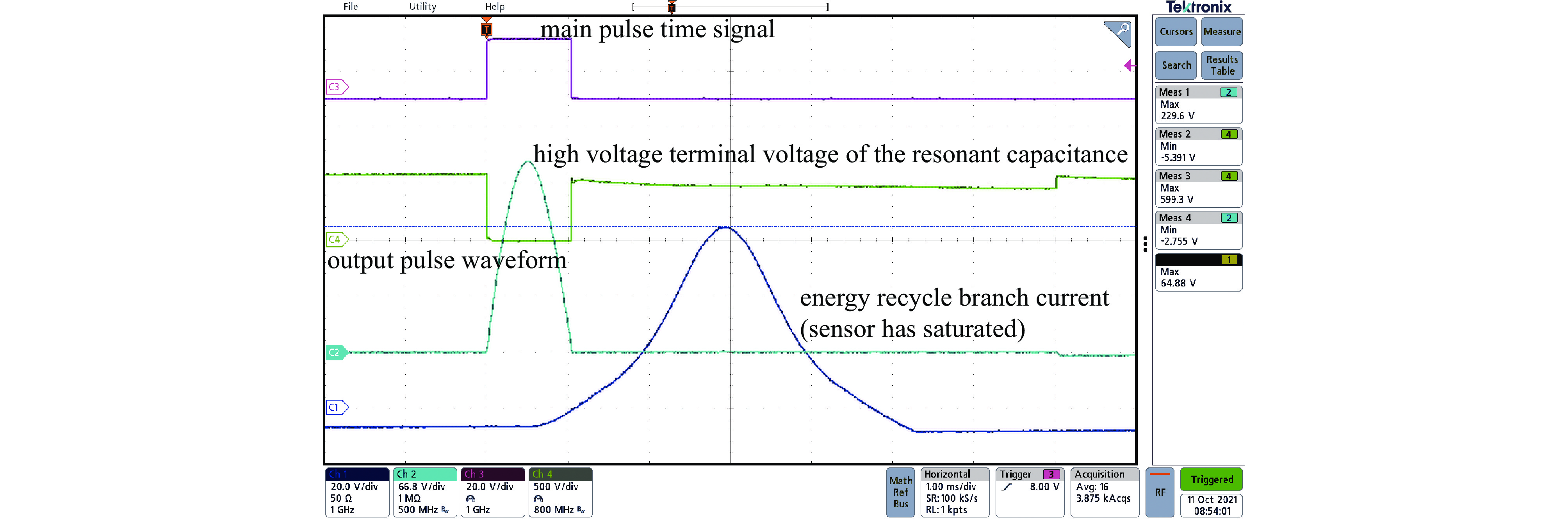
The High Energy Photon Source (HEPS) is the first fourth-generation synchrotron radiation light source in China, including a 6 GeV storage ring, a booster ring and a Linac. As a typical low emittance storage ring (LER), the dynamic aperture of HEPS is far smaller than the physical aperture. Hence, a novel on-axis swap-out injection scheme was chosen. The booster ring accelerates the beam from 500 MeV to 6 GeV. To reduce the extraction kick strength, before injection into the storage ring, four slow bumper magnets are applied to assist the kicker to accomplish extraction. The bumper pulse magnetic field waveform is a half-sine wave with 1ms pulse bottom width. Depending on the simulation and test, a classic LC resonance circuit topology with IGBT switching in series with fast recovery diodes is adopted. Besides, an energy recycle circuit is designed, to decrease power loss and reduce the influence on the output pulse current waveform during the capacitor recharge process. A pulsed power supply prototype is developed, and the testing results show that the bumper pulser can fully meet all the requirements of HEPS booster high energy extraction system.
The High Energy Photon Source (HEPS) is the first fourth-generation synchrotron radiation light source in China, including a 6 GeV storage ring, a booster ring and a Linac. As a typical low emittance storage ring (LER), the dynamic aperture of HEPS is far smaller than the physical aperture. Hence, a novel on-axis swap-out injection scheme was chosen. The booster ring accelerates the beam from 500 MeV to 6 GeV. To reduce the extraction kick strength, before injection into the storage ring, four slow bumper magnets are applied to assist the kicker to accomplish extraction. The bumper pulse magnetic field waveform is a half-sine wave with 1ms pulse bottom width. Depending on the simulation and test, a classic LC resonance circuit topology with IGBT switching in series with fast recovery diodes is adopted. Besides, an energy recycle circuit is designed, to decrease power loss and reduce the influence on the output pulse current waveform during the capacitor recharge process. A pulsed power supply prototype is developed, and the testing results show that the bumper pulser can fully meet all the requirements of HEPS booster high energy extraction system.


2024,
36: 025015.
doi: 10.11884/HPLPB202436.230239
Abstract:
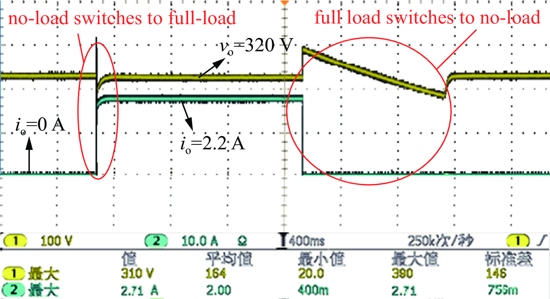
The power supply for fast corrector is an important type of equipment in light sources and accelerators. With the improvement of the performance of the light source, the accelerator has put forward higher requirements for the performance of the fast corrector and their corresponding power supply. To meet the requirements of the power supply for fast corrector and simplify their design process, the research of control strategy and simulation about power supply for the fast corrector is conducted. This paper proposes a way which uses the PI control plus second-order phase compensation as the control strategy of the power supply for fast corrector. For improving the phase margin of the power supply system, Bode diagram is used to design the phase compensation parameters of the power supply fast corrector. This method not only ensures that the power supply system works in the deep negative feedback state, but also simplifies the process of parameter calculation about phase compensation. To verify the correctness and effectiveness of the control strategy, this paper proposes a simulation method based on the transfer function of switching power supply which uses voltage-controlled voltage source instead of switching devices. The simulation results verify the feasibility and effectiveness of the above control strategies, and verify the effectiveness and efficiency of the above simulation methods.
The power supply for fast corrector is an important type of equipment in light sources and accelerators. With the improvement of the performance of the light source, the accelerator has put forward higher requirements for the performance of the fast corrector and their corresponding power supply. To meet the requirements of the power supply for fast corrector and simplify their design process, the research of control strategy and simulation about power supply for the fast corrector is conducted. This paper proposes a way which uses the PI control plus second-order phase compensation as the control strategy of the power supply for fast corrector. For improving the phase margin of the power supply system, Bode diagram is used to design the phase compensation parameters of the power supply fast corrector. This method not only ensures that the power supply system works in the deep negative feedback state, but also simplifies the process of parameter calculation about phase compensation. To verify the correctness and effectiveness of the control strategy, this paper proposes a simulation method based on the transfer function of switching power supply which uses voltage-controlled voltage source instead of switching devices. The simulation results verify the feasibility and effectiveness of the above control strategies, and verify the effectiveness and efficiency of the above simulation methods.


2024,
36: 025016.
doi: 10.11884/HPLPB202436.230194
Abstract:
The primary magnetic field coil (PMFC) power supply system is designed for pumping the PMFC of the kilo-tesla cylindrical implosion magnetic flux compression generator (MC-1) to produce initial magnetic field. It is the key equipment of the MC-1 system. Based on analysis of the requirements and the key techniques, the key components, pulsed forming circuits and control system of the PMFC power supply system were designed. The power supply system with the output voltage adjustable from 1 kV to 40 kV, the rise front about 60 μs and the peak current reached 3.2 MA was developed successfully. The power supply system has been applied to the dynamic test of the kilo-tesla cylindrical implosion magnetic flux compression (MC-1) generator.
The primary magnetic field coil (PMFC) power supply system is designed for pumping the PMFC of the kilo-tesla cylindrical implosion magnetic flux compression generator (MC-1) to produce initial magnetic field. It is the key equipment of the MC-1 system. Based on analysis of the requirements and the key techniques, the key components, pulsed forming circuits and control system of the PMFC power supply system were designed. The power supply system with the output voltage adjustable from 1 kV to 40 kV, the rise front about 60 μs and the peak current reached 3.2 MA was developed successfully. The power supply system has been applied to the dynamic test of the kilo-tesla cylindrical implosion magnetic flux compression (MC-1) generator.


2024,
36: 025017.
doi: 10.11884/HPLPB202436.230228
Abstract:
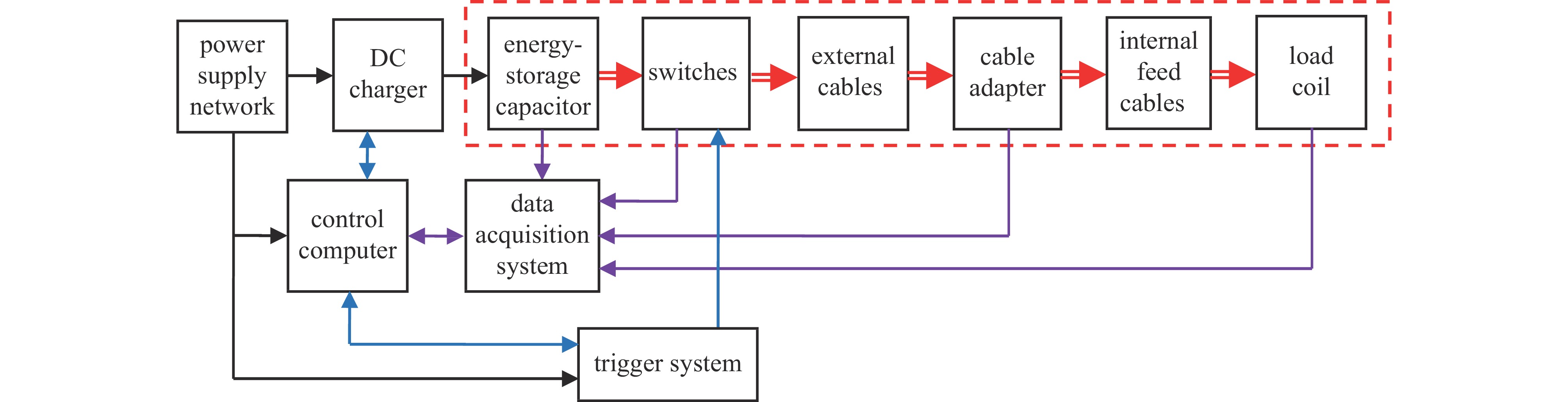
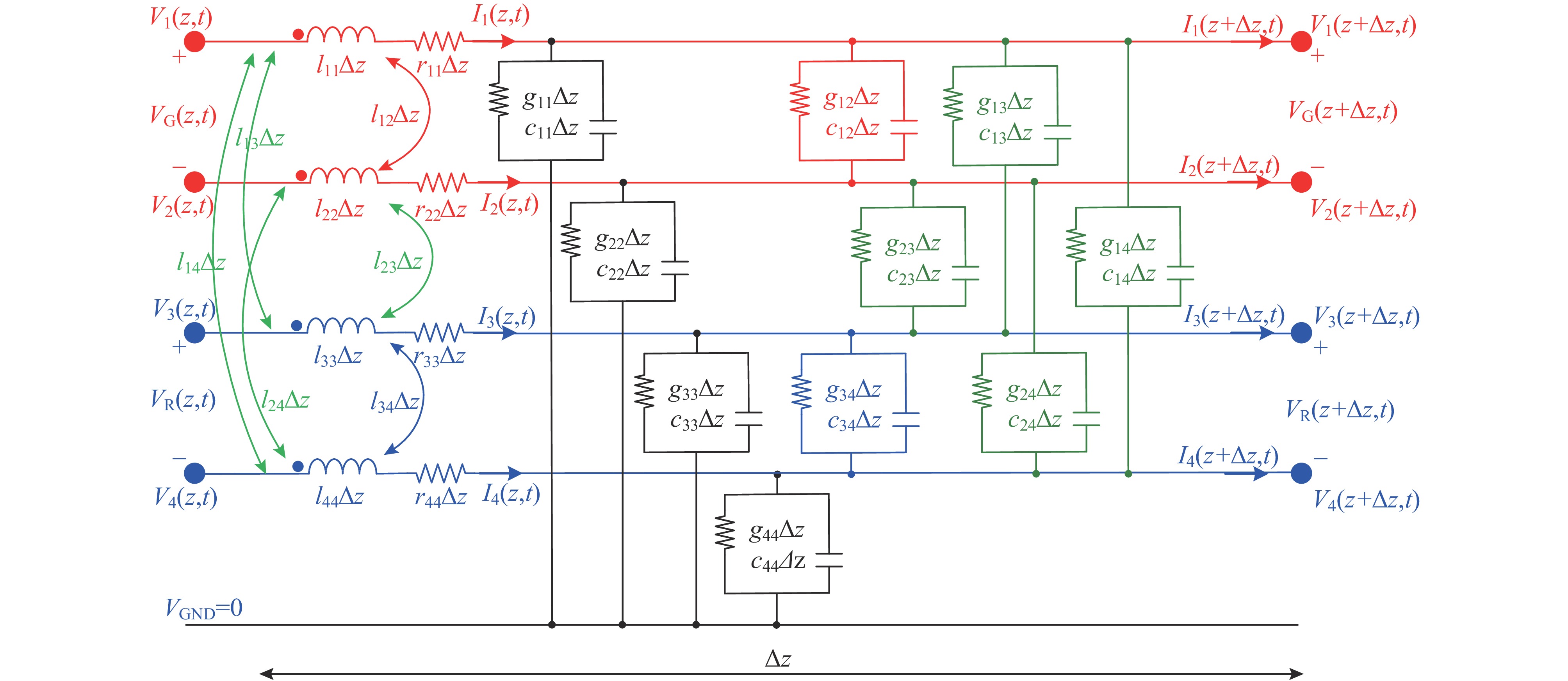
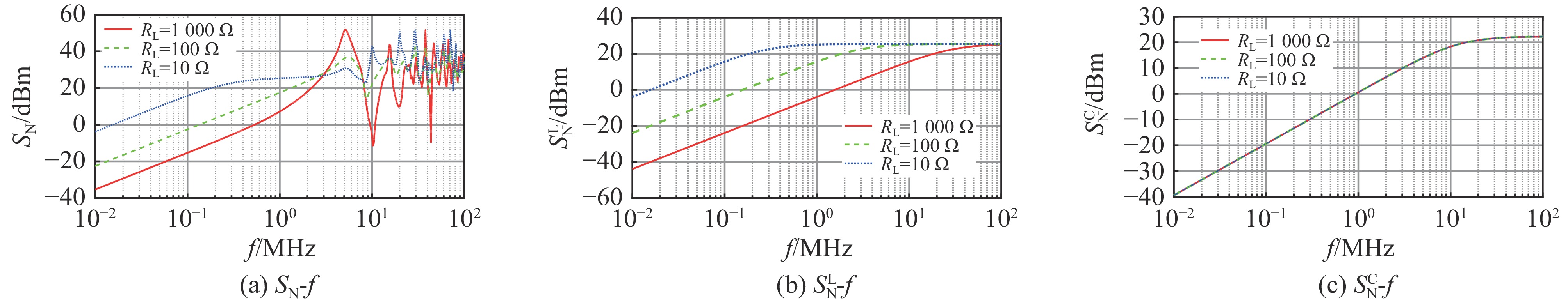
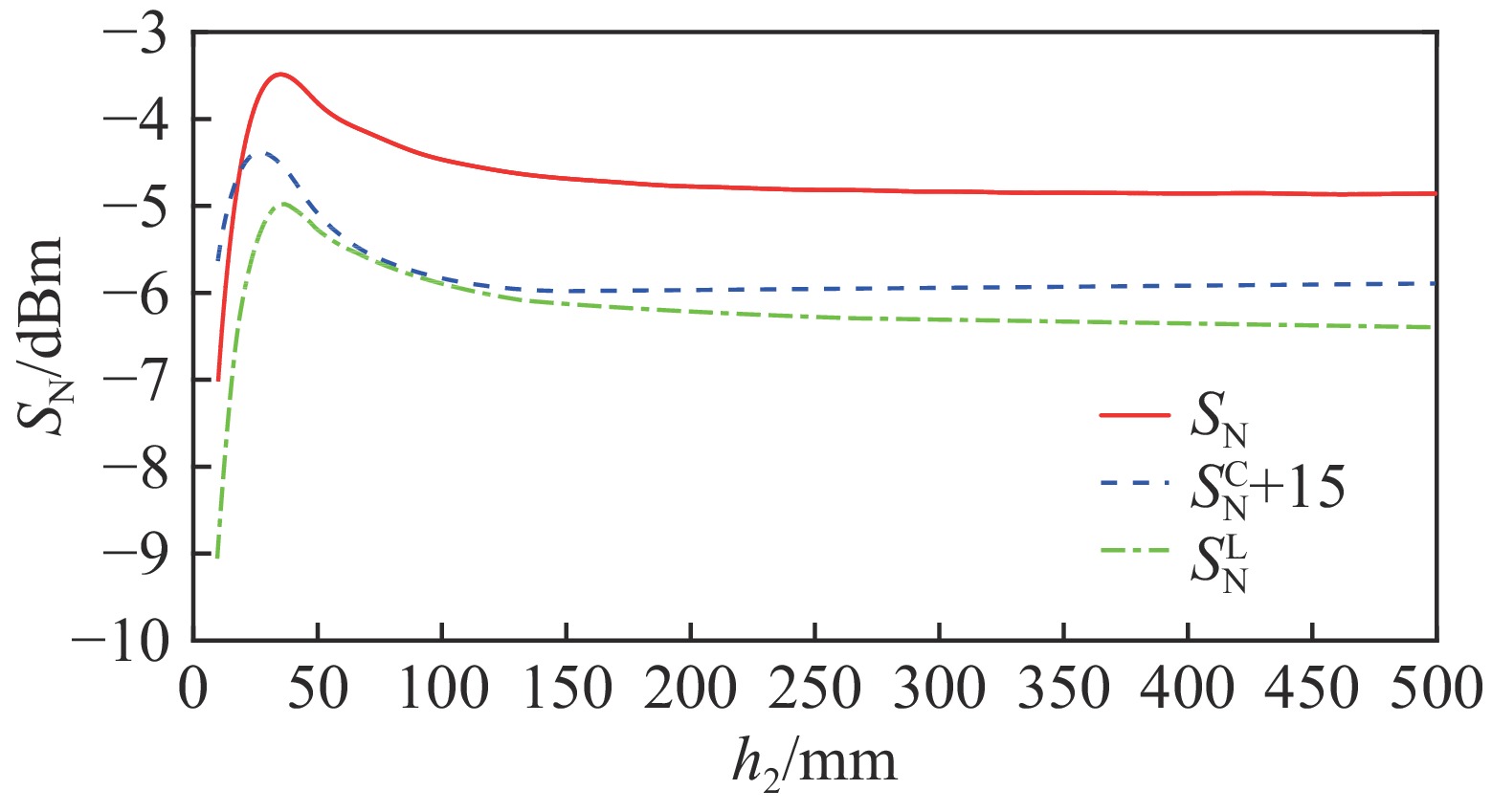
With the development of electrification, it has been paid more and more attention to the electromagnetic compatibility in electrical and electronic systems. To suppress the effects of electromagnetic interference and achieve electromagnetic compatible operation of equipment or components, it is necessary to research the crosstalk between cables. However, few researches have focused on the electromagnetic crosstalk between double differential mode loops consisting of a generator loop, a receptor loop, and the ground. In this paper, a five-conductor transmission line model based on the multi-conductor transmission line theory is proposed, and the crosstalk between double differential mode unshielded cable loops is researched based on it. According to the coupling mechanism, the method firstly establishes the equivalent model of unit-length five-conductor transmission line, then writes the system of Kirchhoff equations according to the method of finite difference, and finally solves the equations after supplementing the boundary conditions to obtain the crosstalk in the frequency domain. The crosstalk calculation results are compared with the simulation results of CST software to verify the feasibility and validity of the model and calculation method. The inductive coupling and capacitive coupling are studied respectively by the calculation, and the influence laws of different factors on the cable crosstalk are obtained by calculation and analysis, which can provide guidance for taking measures to suppress cable crosstalk in practical engineering.
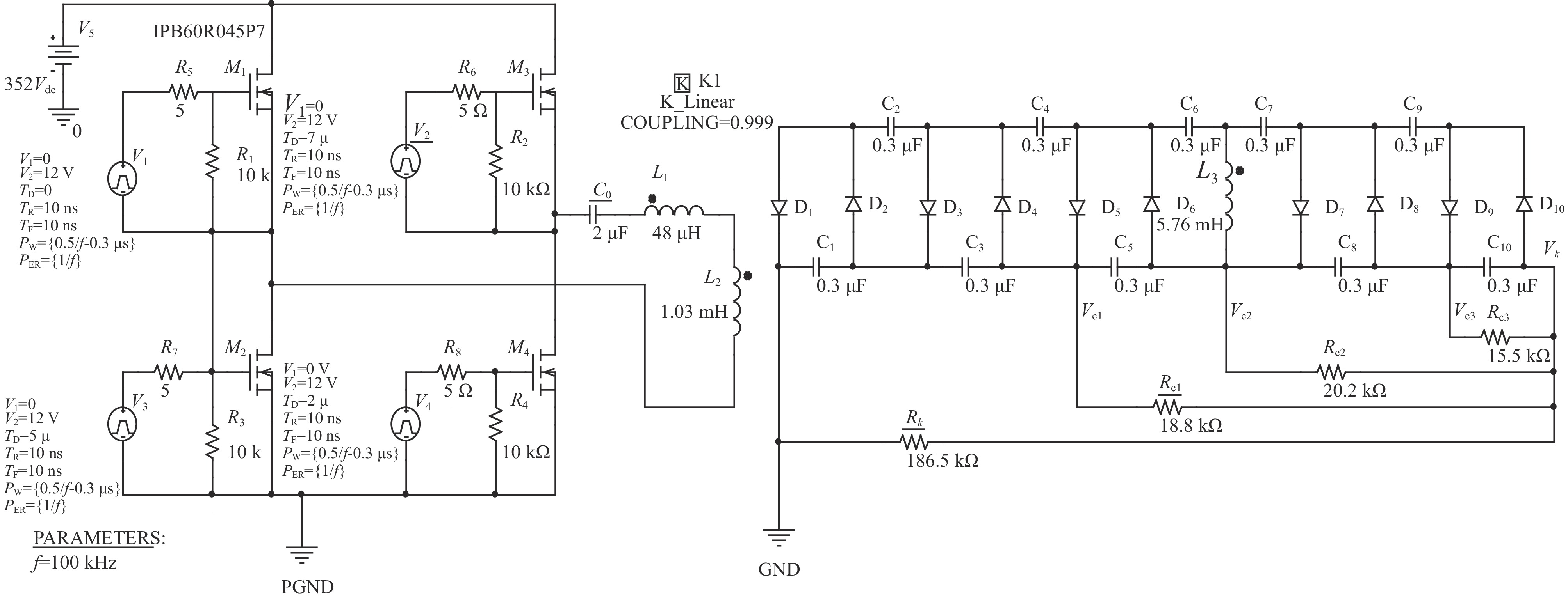
With the development of electrification, it has been paid more and more attention to the electromagnetic compatibility in electrical and electronic systems. To suppress the effects of electromagnetic interference and achieve electromagnetic compatible operation of equipment or components, it is necessary to research the crosstalk between cables. However, few researches have focused on the electromagnetic crosstalk between double differential mode loops consisting of a generator loop, a receptor loop, and the ground. In this paper, a five-conductor transmission line model based on the multi-conductor transmission line theory is proposed, and the crosstalk between double differential mode unshielded cable loops is researched based on it. According to the coupling mechanism, the method firstly establishes the equivalent model of unit-length five-conductor transmission line, then writes the system of Kirchhoff equations according to the method of finite difference, and finally solves the equations after supplementing the boundary conditions to obtain the crosstalk in the frequency domain. The crosstalk calculation results are compared with the simulation results of CST software to verify the feasibility and validity of the model and calculation method. The inductive coupling and capacitive coupling are studied respectively by the calculation, and the influence laws of different factors on the cable crosstalk are obtained by calculation and analysis, which can provide guidance for taking measures to suppress cable crosstalk in practical engineering.


2024,
36: 025018.
doi: 10.11884/HPLPB202436.230155
Abstract:
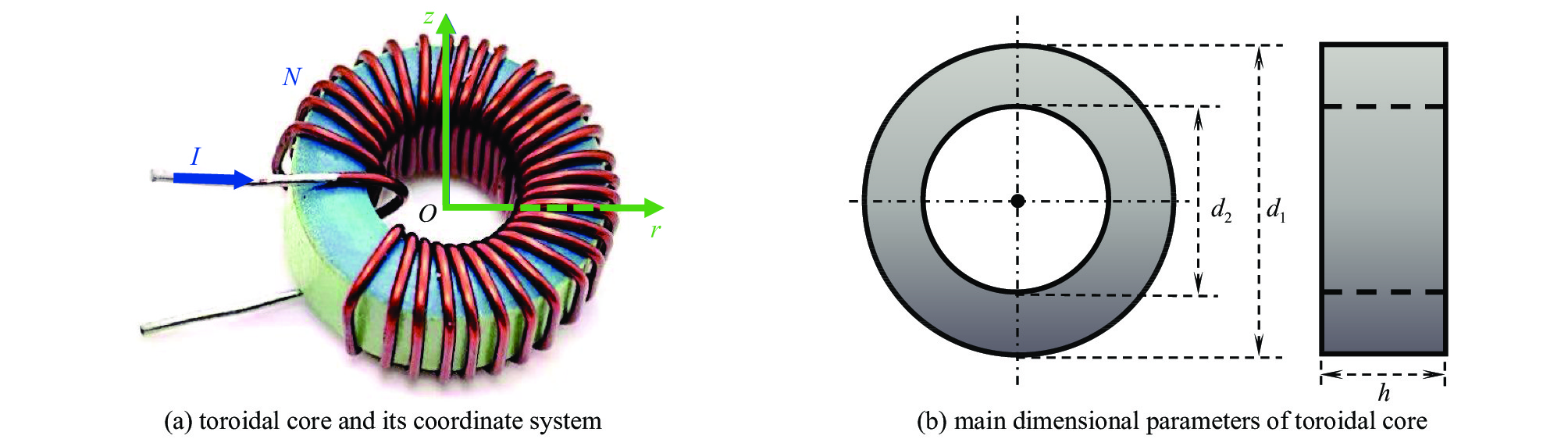
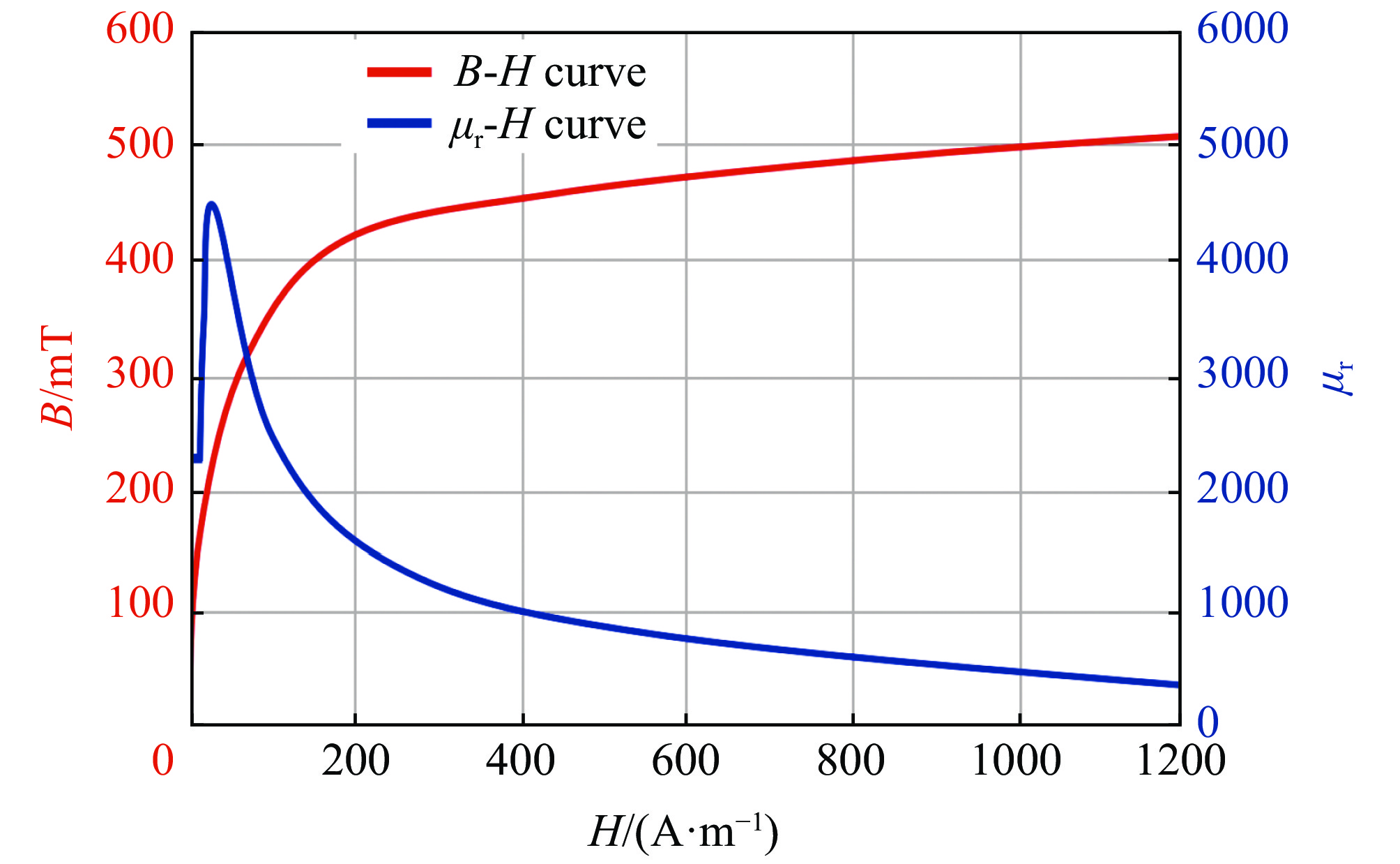
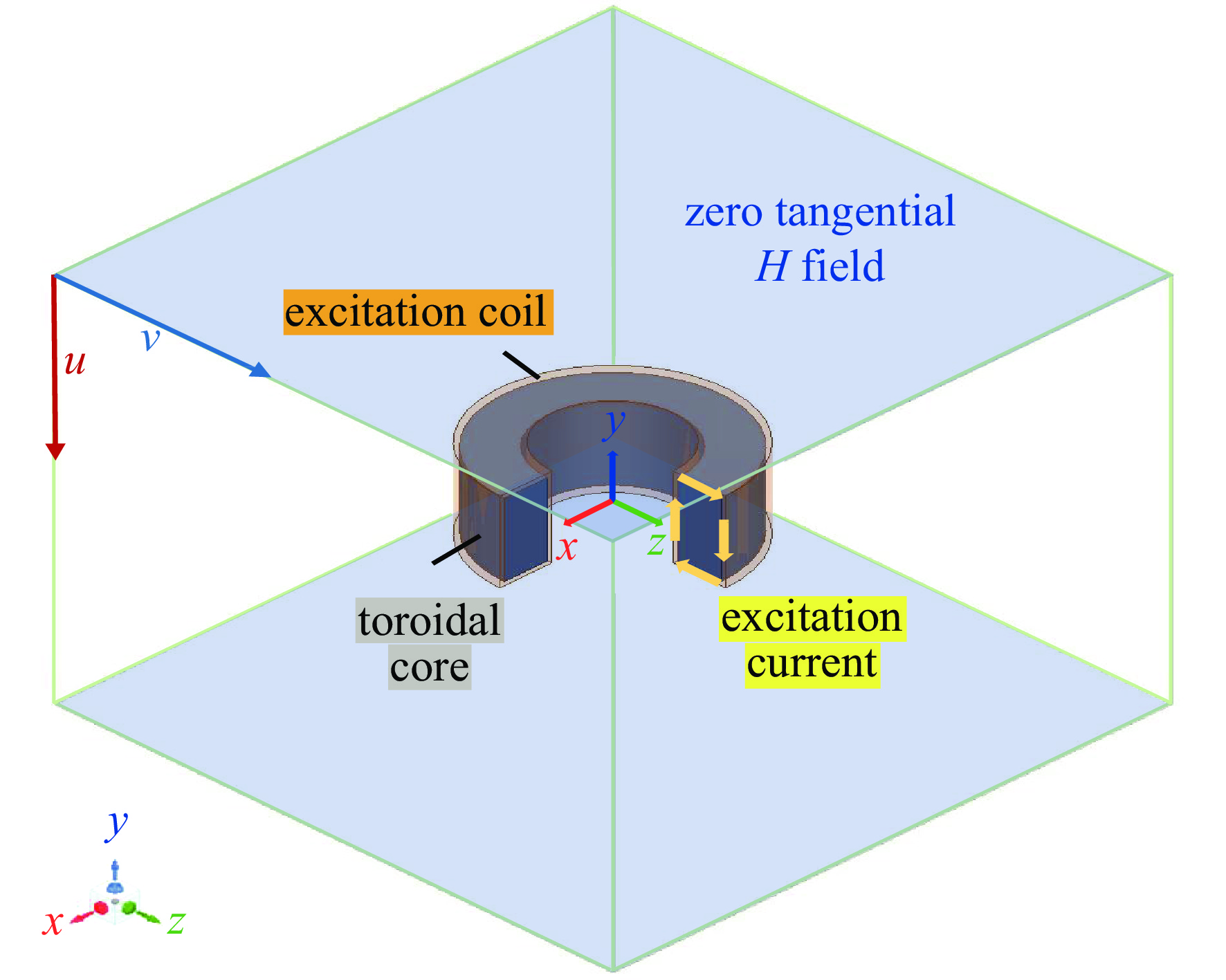
The magnetic components in power supplies are naturally sensitive to external magnetic fields, and their operating characteristics directly affect the output characteristics of the power supply. Modeling the background magnetic field is an important prerequisite for the study of the interference of magnetic components in power supplies by strong stray magnetic fields, but few studies have focused on this application scenario, and the commonly used methods for electromagnetic field analysis are difficult to balance accuracy and efficiency. In this paper, we propose a method to analyze the influence of stray magnetic fields based on the equivalent magnetic circuit network method, which discrete the research object into magnetic circuit units, equivalently form a network model, and obtain the field distribution of the model by solving the equations of the equivalent magnetic circuit system. We take a toroidal ferrite core as an example, and use the equivalent circuit network method to calculate the field distribution of the toroidal core under DC excitation and uniform orthogonal magnetic field, and analyze the effect of the background magnetic field on its equivalent inductance. By comparing the results of the equivalent circuit network method with those of the finite element method, the accuracy and efficiency of the proposed analysis method are demonstrated, and it is shown that the method is applicable to the analysis of power supplies disturbed by the background magnetic field.
The magnetic components in power supplies are naturally sensitive to external magnetic fields, and their operating characteristics directly affect the output characteristics of the power supply. Modeling the background magnetic field is an important prerequisite for the study of the interference of magnetic components in power supplies by strong stray magnetic fields, but few studies have focused on this application scenario, and the commonly used methods for electromagnetic field analysis are difficult to balance accuracy and efficiency. In this paper, we propose a method to analyze the influence of stray magnetic fields based on the equivalent magnetic circuit network method, which discrete the research object into magnetic circuit units, equivalently form a network model, and obtain the field distribution of the model by solving the equations of the equivalent magnetic circuit system. We take a toroidal ferrite core as an example, and use the equivalent circuit network method to calculate the field distribution of the toroidal core under DC excitation and uniform orthogonal magnetic field, and analyze the effect of the background magnetic field on its equivalent inductance. By comparing the results of the equivalent circuit network method with those of the finite element method, the accuracy and efficiency of the proposed analysis method are demonstrated, and it is shown that the method is applicable to the analysis of power supplies disturbed by the background magnetic field.


2024,
36: 025019.
doi: 10.11884/HPLPB202436.230212
Abstract:
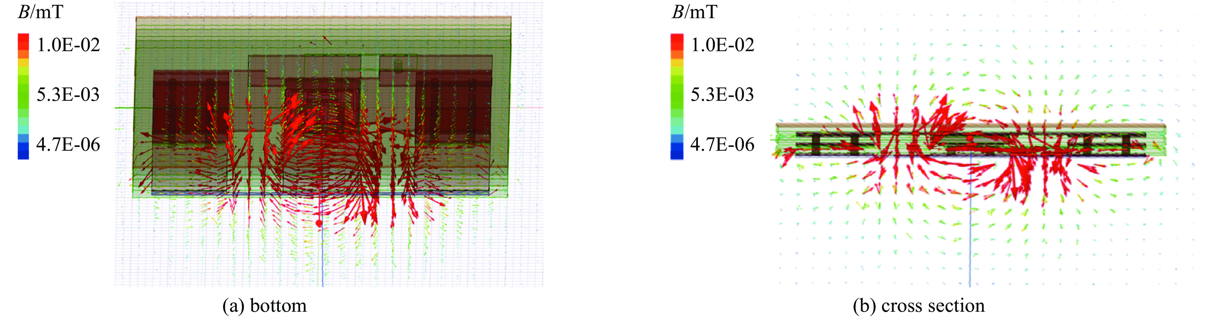
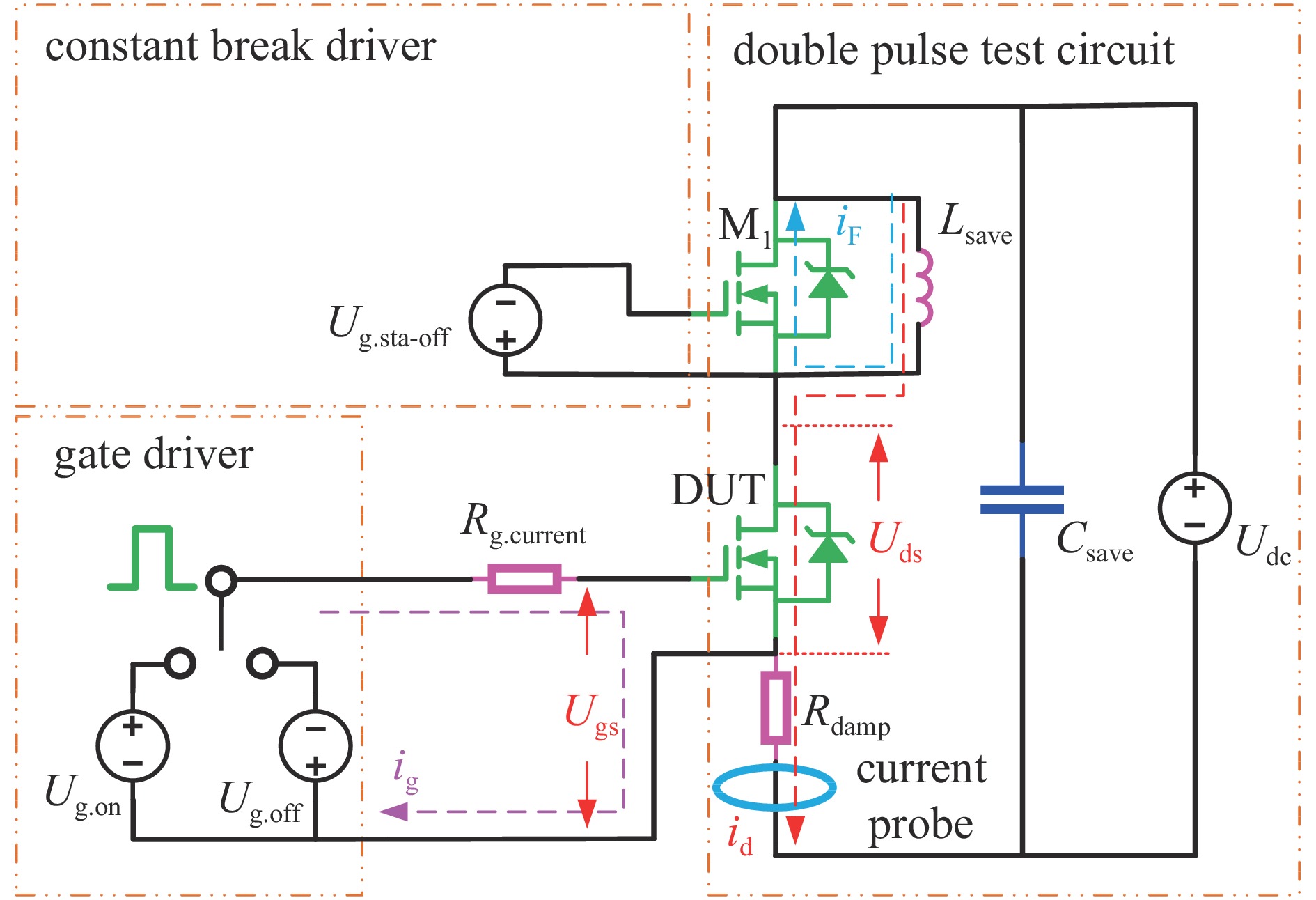
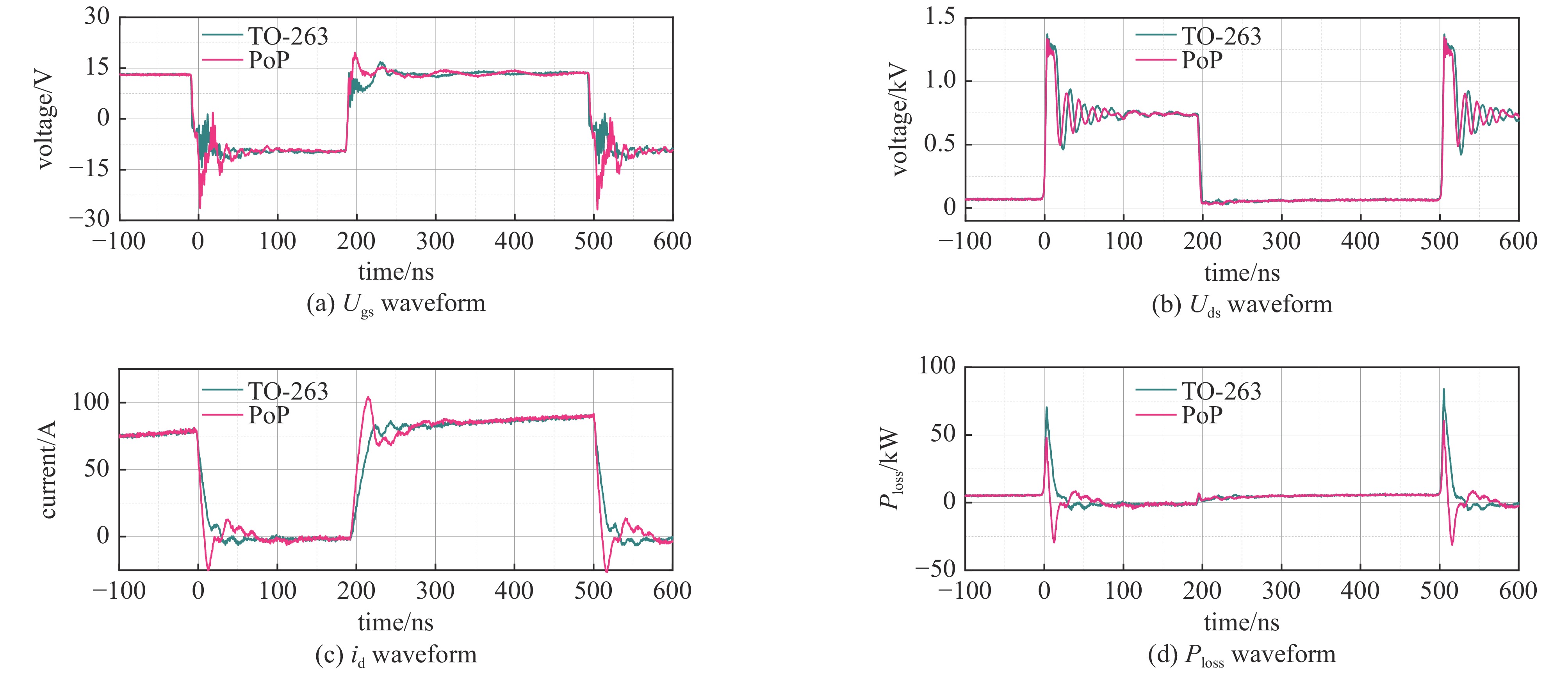
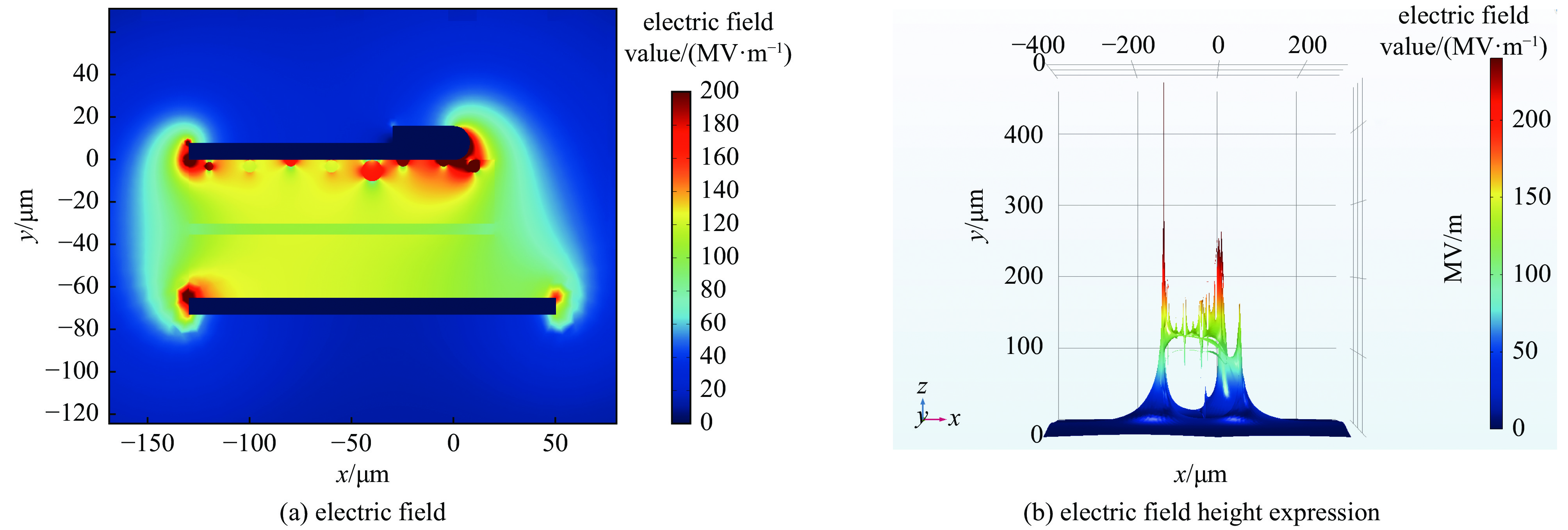
As the core component of pulse power system, switch plays an important role in pulse forming and power modulation. Usually, the rise time of the pulse generated is determined by the on-off speed of switch and the high-speed switch is vital to the formation of nanosecond short pulses. Therefore, this paper proposes a high-speed SiC-MOSFET package on package structure. The overall layout has no lead or external connection, and has very low parasitic inductance. In this paper, the electromagnetic field simulation research of the proposed package is carried out, and the electromagnetic field distribution of the multi-media interface of the package is revealed during the pulse formation process. The electromagnetic weak link of the package structure is clarified, which provides guidance for further insulation optimization. A dual-pulse test platform was built to compare the dynamic performance of the proposed package-on-package structure switch and the commercial TO-263-7 package switch. The experimental results show that under high current conditions, the proposed packaging improves the turnning off by 48%, the turnning off speed by 50%, the turnning on loss by 54.6%, and the turnning off loss by 62.8%. The experimental results verify the improvement effect of the package-on-package structure on the switch dynamic performance.
As the core component of pulse power system, switch plays an important role in pulse forming and power modulation. Usually, the rise time of the pulse generated is determined by the on-off speed of switch and the high-speed switch is vital to the formation of nanosecond short pulses. Therefore, this paper proposes a high-speed SiC-MOSFET package on package structure. The overall layout has no lead or external connection, and has very low parasitic inductance. In this paper, the electromagnetic field simulation research of the proposed package is carried out, and the electromagnetic field distribution of the multi-media interface of the package is revealed during the pulse formation process. The electromagnetic weak link of the package structure is clarified, which provides guidance for further insulation optimization. A dual-pulse test platform was built to compare the dynamic performance of the proposed package-on-package structure switch and the commercial TO-263-7 package switch. The experimental results show that under high current conditions, the proposed packaging improves the turnning off by 48%, the turnning off speed by 50%, the turnning on loss by 54.6%, and the turnning off loss by 62.8%. The experimental results verify the improvement effect of the package-on-package structure on the switch dynamic performance.


2024,
36: 025020.
doi: 10.11884/HPLPB202436.230163
Abstract:
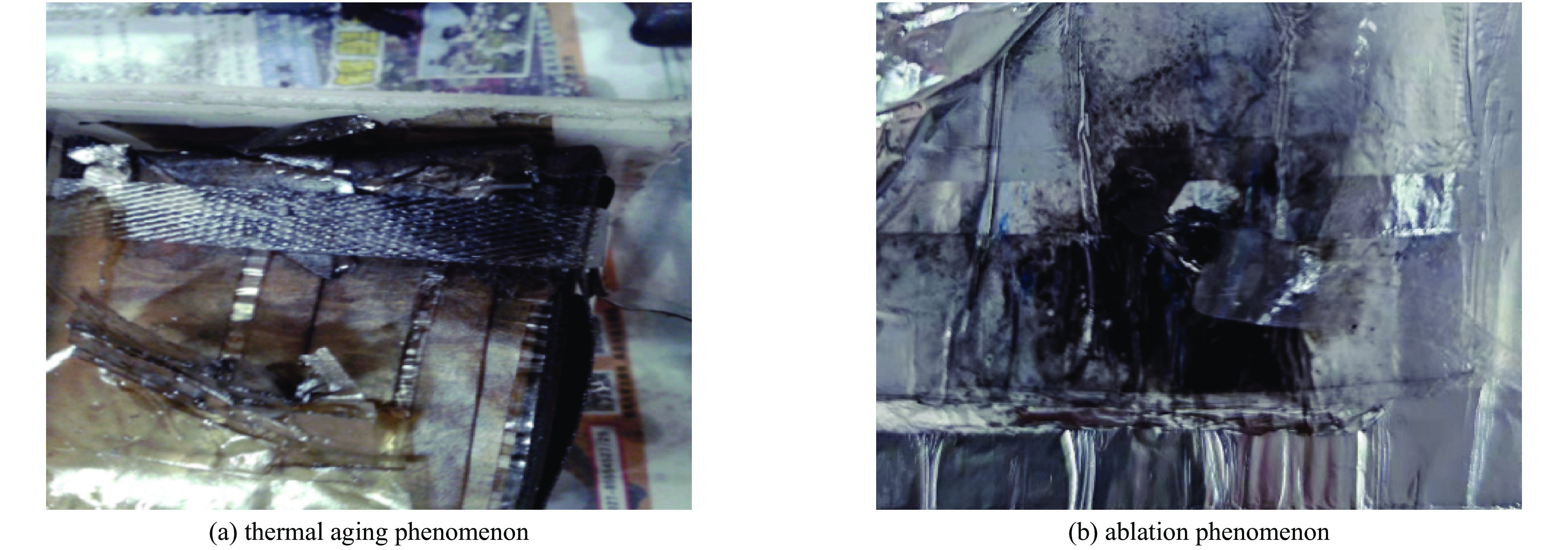
The all-film pulsed capacitor is an important energy storage unit of the pulsed power system, and its lifetime affects the reliability of the whole system. Under the pulse condition, the failure of the all-film pulsed capacitor is mostly a sudden failure, and the life is highly dispersed. To explore the aging and failure mechanism of all-film pulsed capacitors, the life test and the simulation of electric and temperature fields were carried out. The life test of the capacitor was carried out by using the LTD basic discharge unit (brick) experimental chamber to test the life of the capacitor and obtain the failed capacitor, and the failure causes of the failed capacitor under different fault forms were analyzed, and the electric field simulation of the local “electric field distortion” area of the capacitor was carried out by using the finite element analysis software, which showed that the distorted electric field in the above area was the main reason for the breakdown of the insulating medium. The temperature field analysis of the capacitor shows that the temperature of the capacitor is positively correlated with the charge-discharge frequency, and the highest temperature point is located near the geometric center of the capacitor, and the temperature rise of the capacitor is not obvious when the charge-discharge frequency is low, indicating that the aging of the capacitor insulating medium is mainly electrical aging rather than thermal aging at low charge-discharge frequency.
The all-film pulsed capacitor is an important energy storage unit of the pulsed power system, and its lifetime affects the reliability of the whole system. Under the pulse condition, the failure of the all-film pulsed capacitor is mostly a sudden failure, and the life is highly dispersed. To explore the aging and failure mechanism of all-film pulsed capacitors, the life test and the simulation of electric and temperature fields were carried out. The life test of the capacitor was carried out by using the LTD basic discharge unit (brick) experimental chamber to test the life of the capacitor and obtain the failed capacitor, and the failure causes of the failed capacitor under different fault forms were analyzed, and the electric field simulation of the local “electric field distortion” area of the capacitor was carried out by using the finite element analysis software, which showed that the distorted electric field in the above area was the main reason for the breakdown of the insulating medium. The temperature field analysis of the capacitor shows that the temperature of the capacitor is positively correlated with the charge-discharge frequency, and the highest temperature point is located near the geometric center of the capacitor, and the temperature rise of the capacitor is not obvious when the charge-discharge frequency is low, indicating that the aging of the capacitor insulating medium is mainly electrical aging rather than thermal aging at low charge-discharge frequency.


2024,
36: 025021.
doi: 10.11884/HPLPB202436.230171
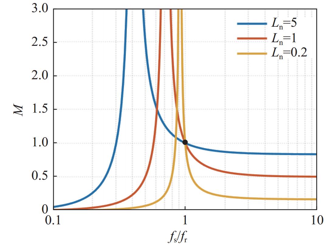
Abstract:
With the continuous development of aerospace technology, the demand for Hall-electric propulsion power processing units (PPUs) in spacecraft is constantly increasing, and high-gain, high-power and high-efficiency PPUs have become the mainstream direction of research. The LLC topology enables soft switching over the full load range and therefore offers broad application prospects in PPU anode power supplies. Due to its primary and secondary gain characteristics, the primary LLC brings great challenges to the resonant inductance design of the high gain converter of the anode power supply. In view of the above problems, this paper proposes an improved secondary LLC resonant topology, which retains the soft switching characteristics of the primary LLC resonant circuit while effectively solving the resonant inductor design problem, so that the PPU anode power supply has high gain performance. In this paper, the mathematical model of the secondary LLC topology is first established by using the time domain analysis method, and then the calculation method of the peak gain is given on the basis of the model, and finally the correctness of the built model is verified by a prototype and the validity of the secondary LLC circuit is verified.
With the continuous development of aerospace technology, the demand for Hall-electric propulsion power processing units (PPUs) in spacecraft is constantly increasing, and high-gain, high-power and high-efficiency PPUs have become the mainstream direction of research. The LLC topology enables soft switching over the full load range and therefore offers broad application prospects in PPU anode power supplies. Due to its primary and secondary gain characteristics, the primary LLC brings great challenges to the resonant inductance design of the high gain converter of the anode power supply. In view of the above problems, this paper proposes an improved secondary LLC resonant topology, which retains the soft switching characteristics of the primary LLC resonant circuit while effectively solving the resonant inductor design problem, so that the PPU anode power supply has high gain performance. In this paper, the mathematical model of the secondary LLC topology is first established by using the time domain analysis method, and then the calculation method of the peak gain is given on the basis of the model, and finally the correctness of the built model is verified by a prototype and the validity of the secondary LLC circuit is verified.


2024,
36: 025022.
doi: 10.11884/HPLPB202436.230233
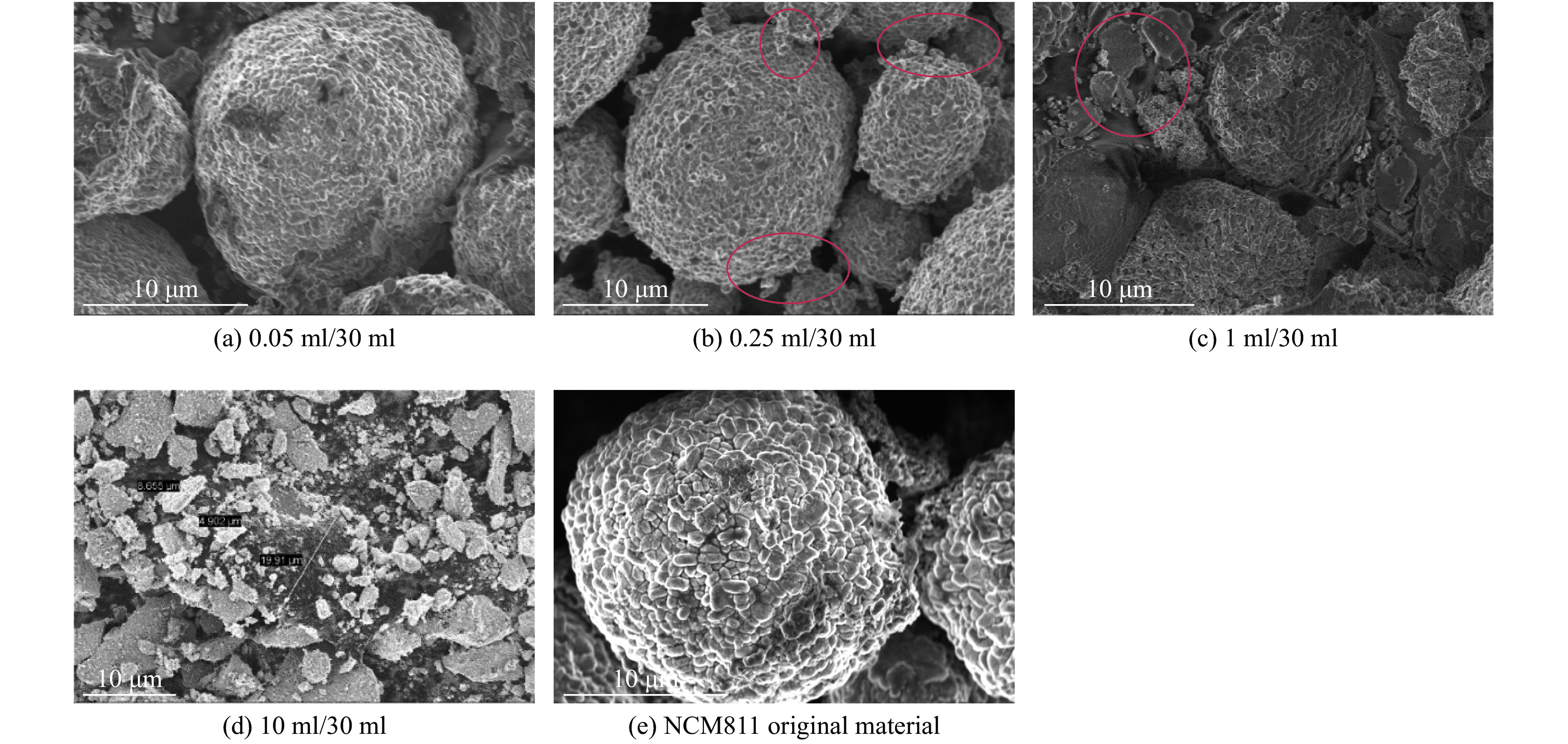
Abstract:
High nickel materials have good electrochemical performance, but there is a problem of poor surface stability. In this study, tetrabutyl titanate was hydrolyzed on the surface of NCM811 material to generate TiO2. SEM and TEM analysis results indicate that the TiO2 layer can be uniformly coated on the surface of high nickel NCM811 using the proposed method. By utilizing the combined effect of surface coating and bulk doping, the capacity retention rate of the material increased from 81.40% to 92.39% after 200 cycles under 1C discharge condition, and the electrochemical performance of NCM811 material was improved.
High nickel materials have good electrochemical performance, but there is a problem of poor surface stability. In this study, tetrabutyl titanate was hydrolyzed on the surface of NCM811 material to generate TiO2. SEM and TEM analysis results indicate that the TiO2 layer can be uniformly coated on the surface of high nickel NCM811 using the proposed method. By utilizing the combined effect of surface coating and bulk doping, the capacity retention rate of the material increased from 81.40% to 92.39% after 200 cycles under 1C discharge condition, and the electrochemical performance of NCM811 material was improved.