Loading [MathJax]/jax/output/SVG/jax.js

留言板

尊敬的读者、作者、审稿人, 关于本刊的投稿、审稿、编辑和出版的任何问题, 您可以本页添加留言。我们将尽快给您答复。谢谢您的支持!

姓名
邮箱
手机号码
标题
留言内容
验证码

Analysis of modules failure in solid-state amplifier for high current RFQ

Sun Liepeng Yuan Zhenyu Zhang Cheng Shi Longbo Miao Jungang Zhang Jianhua Xu Xianbo He Yuan

Sun Liepeng, Yuan Zhenyu, Zhang Cheng, et al. Analysis of modules failure in solid-state amplifier for high current RFQ[J]. High Power Laser and Particle Beams, 2019, 31: 065103. doi: 10.11884/HPLPB201931.180245
Citation: Sun Liepeng, Yuan Zhenyu, Zhang Cheng, et al. Analysis of modules failure in solid-state amplifier for high current RFQ[J]. High Power Laser and Particle Beams, 2019, 31: 065103. doi: 10.11884/HPLPB201931.180245
孙列鹏, 袁震宇, 张诚, 等. 强流RFQ的固态功率源模块故障分析[J]. 强激光与粒子束, 2019, 31: 065103. doi: 10.11884/HPLPB201931.180245
引用本文: 孙列鹏, 袁震宇, 张诚, 等. 强流RFQ的固态功率源模块故障分析[J]. 强激光与粒子束, 2019, 31: 065103. doi: 10.11884/HPLPB201931.180245

Analysis of modules failure in solid-state amplifier for high current RFQ

Funds: 

Strategic Priority Research Program of Chinese Academy of Sciences XDA030205

More Information
    Author Bio:

    Sun Liepeng(1979—), PhD, senior engineer, majors in RF system technology and electromagnetic field; sunnyslp@163.com

强流RFQ的固态功率源模块故障分析

doi: 10.11884/HPLPB201931.180245
基金项目: 

Strategic Priority Research Program of Chinese Academy of Sciences XDA030205

详细信息
  • 中图分类号: TN242

  • 摘要: 用于中科院近代物理研究所的ADS项目中的射频四极加速器(RFQ) 的新RF系统在2017年初升级,原来的电子四极放大器被两个新的固态功放(SSA) 所替换,它们是两台相同的额定功率为80 kW的功率源,通过两个相同的耦合器在腔内合成至少100 kW的功率。但是对于SSA来说,为了功率组合,太多的功率模块的振幅和相位进行了调整和优化,一个或几个损坏的环形器(包括吸收负载) 可能导致整个射频系统的失效。特别是,根据实验和仿真,发生失配问题后,如果两级合成器之间的传输线电长度满足某一特定条件时,系统的散射参数会有很大的波动,甚至切断。详细介绍了北京北广科技股份有限公司用于模拟多级合成放大的模拟方法、放大链路的故障分析及相关实验情况。
  • Since the old 200 kW tetrode amplifier had been operating in high current beam of a Radio Frequency Quadrupole (RFQ) cavity without a circulator for more than two years, two new solid-state amplifiers (SSAs), which can operate under the full mismatch condition for a time period as long as several hours, were considered to replace it on site due to their specialties of anti-reflection. SSA is very attractive for individually driven independently phased cavities in proton linear accelerators, because it has such features of MOSFETs like linearity, low noise, high efficiency, high reliability, low cost and long lifetime.

    RFQ cavity operates at 162.5 MHz, the dissipated power reaches up to approximately 90 kW, and especially, the beam power was 21 kW while 10 mA beam current was applied[1]. In Beijing Broadcast Equipment Factory (BBEF) design of amplifier, we found the solution of a distributed protection cheaper than the one with a big circulator and an RF termination at the amplifier output. Thus, a power circulator and an RF termination are included inside every module to protect the MOSFET against excess reflected power. Furthermore, some special technologies of new generation SSA were developed for this kind of high intensity accelerator, such as two types of reflection power experiments on module including long-term continuous wave power and four times pulsed power within 20 ms. Due to the very high power, the design of power module and combiner need to optimize the scattering parameters in the case of mismatch resulting from the multi-port balance or cavity sparking.

    In addition, Low Level RF system (LLRF) must adjust the offsets of output gain and phase due to the different output characteristics from two amplifiers of different manufacturers, BBEF Science & Technology Co. Ltd and Chengdu Kaiteng Sifang Digital Radio & TV Equipment Co. Ltd. The operating mode of this kind of RF system, whose RF power on two identical couplers comes from different amplifiers, implies the balance output power gain and phase be considered at the same time, so that the attenuator and phase shifter were adjusted carefully for the nominal power output and linear region amplification[2].

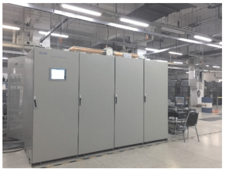
    In order to sum the power coming from over 120 modules, several level synthesizers are used for full power output, which is shown in Fig. 1, and every module can provide a maximum of 850 W RF power for the nominal power even when one pre-amplifier fails. Thus, the tuning process of amplitude and phase from the modules was very complicated due to too many modules. All the modules have been individually tested before combining them. Several tests were carried out by using a network analyzer to determine the S-parameters at low power as well as a power meter, an oscilloscope and a spectrum analyzer to measure characteristics at high power. In the latter case the monitoring devices were connected either to a directional coupler between the module and the load or to a high-power attenuator.

    Figure  1.  The overview of BBEF 80 kW solid-state amplifier

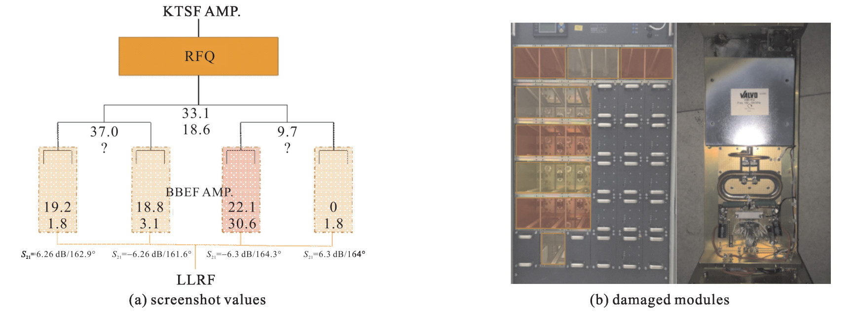
    At a serious accident of June 2017, 19 power modules were burned simultaneously. Almost all power transistors, circulators and sink loads (connected directly with the circulators) in these modules were damaged seriously and must be replaced. When failure happened, the power values were recorded from the monitoring system shown in the screen of a control system, as were presented in Fig. 2 (a). Fig. 2 (b) is a photo of the damaged modules.

    Figure  2.  The screenshot values when failure happened (a) and the damaged modules (b) in the amplifier

    During the operation, the two SSAs were both consisted of four 19″(48.26 cm) racks to integrate gradually, each rack could provide 50 or 60 kW RF power (without beam or with 10 mA CW beam) for separate coupler at the same time. Before basic analysis and check on the machine, one possible reason of accident should be the highly sensitive driving signal interlock in the third section compared to the other three racks, the input signal of the third section was shut down suddenly because of abnormal interlock during the operation, the other three sections were influenced to increase power rapidly at that time due to LLRF close loop on the amplitude modulation. Furthermore, the weird (all at left side of the third section) location of all damaged modules indicates that some inappropriate RF configuration needs to be modified and optimized.

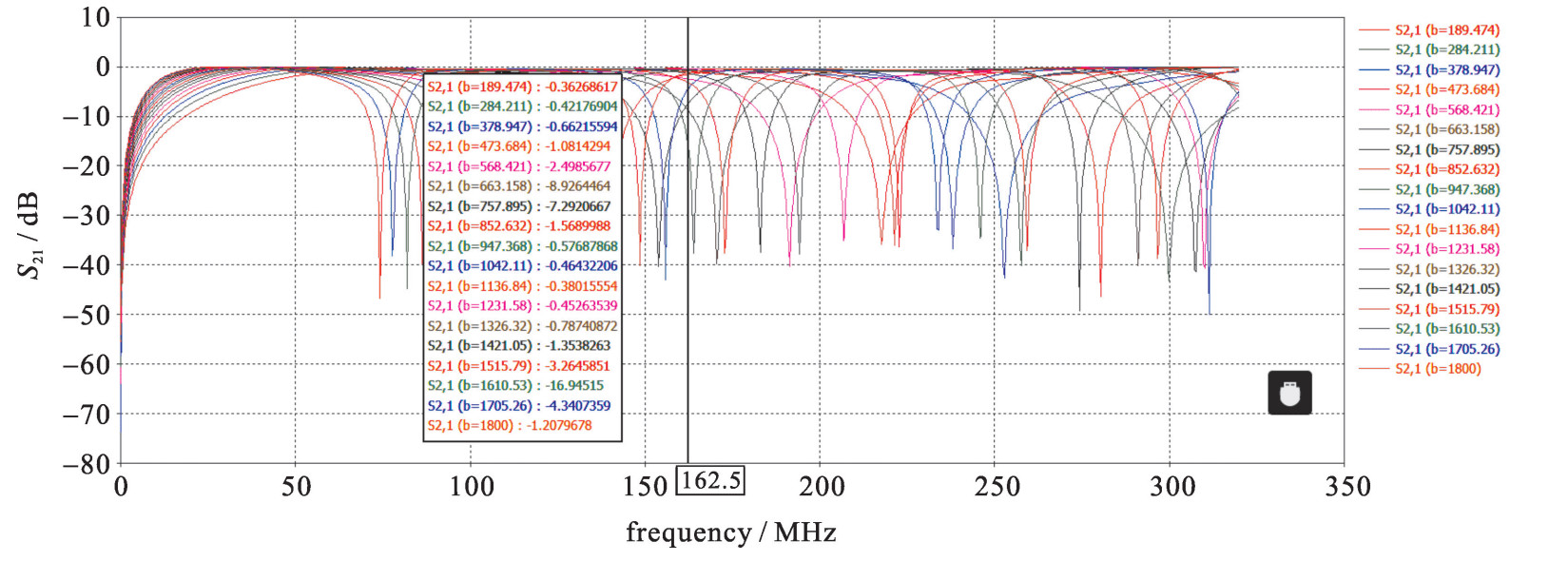
    For the convenience of analysis, a corresponding model of a multi-port power combiner was created in simulation software Microwave Studio to figure out the variation regularities of the scattering parameter. According to the simulated results, if any one port was open or short, the parameter S21 along transmission line on the port had a very great fluctuation along the whole phase range, even when the wavelength moved to a certain value, the scattering parameter would take dramatic turn to block the RF signal. Fig. 3 shows the sweep results in CST simulation, which indicates there are some reflected power points to block the power through combiners when one or a couple of ports fail.

    Figure  3.  The simulated results focus on the wavelength influence from mismatch port

    Generally, one advantage of SSA is continuing output while one or some modules fail, however, the output power decreases. For instance, n modules fail in a 6 kW combiner with 8 modules, the output power is degraded (8-n)2/82×100%. The situation would be much complicated while the circulators inside the module were broken rather than the field-effect transistors. The analysis of n ports network is gained through the degraded matrix[3], Sm=S+SГ(I-S)-1S [4] (the roman letter subscripts represent different sections, n ports connect to arbitrary loads, in which m ports deal with no load, i.e., full reflection). According to symmetry and lossless combination of nine ports device, the matrix of a 8-1 combiner is

    S=[78181818181818181818781818180](99) (1)

    thus its degraded matrix while mismatch (full reflection) is

    S=[164e2φi+5678164e2φi+56+78164e2φi+56+78232e2φi+28+24164e2φi+56+78164e2φi+56+78232e2φi+28+24232e2φi+28+24232e2φi+28+2418e2φi+7](88) (2)

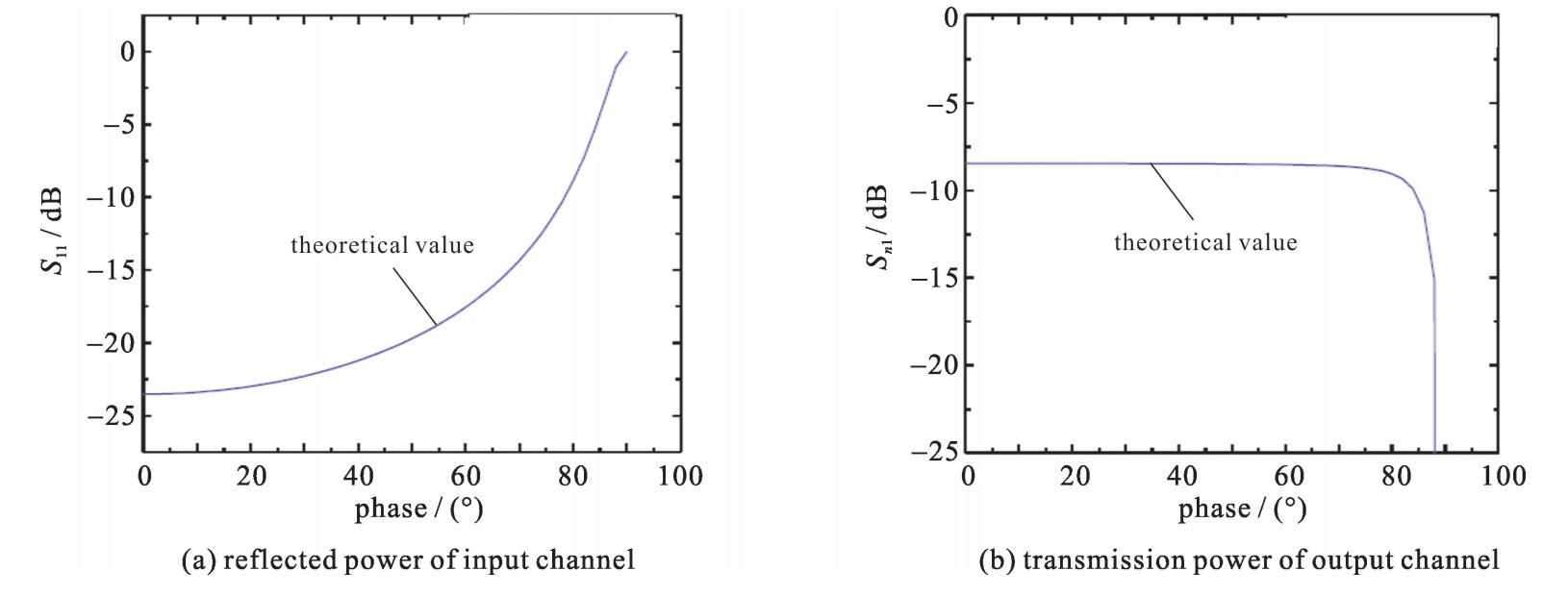
    When one output port was short, the degenerate matrix[5] can be deduced Eq.(2). So, when the phase of short port was 0 or π, the minimum S11 (S11 is reflection of the first port, while Sn1 represents transmission of the nth port) of 0.066 7 and reflected power of input port would be gained simultaneously; when the phase was 90°, S11 got the maximum value of -1 to mean the full power reflection[6]. The S11 and Sn1 were plotted in Fig. 4 according to the matrix of Eq.(2).

    Figure  4.  The simulation focused on the wavelength influence from the phase

    Obviously, the results from Eq.(2) had a good agreement with the CST simulated ones. Then a targeted experiment was prepared for this situation, which took advantage of a three-level combiner/ divider to measure the scattering parameter while any one port mismatched (short or open circuit). An 8-way combiner/ divider was designed and manufactured into a three-level circuit for the purpose of changing the wavelength between the different levels in Fig. 5.

    Figure  5.  A special three-stage combiner for the measurements during module failure

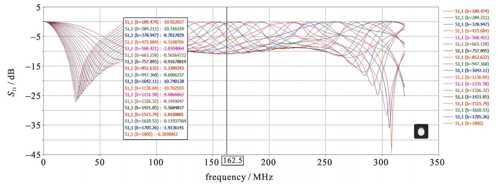
    For these three-level combiners[7], the failure of one port would lead to change greatly, even block RF signal completely. According to the rule of scattering parameter, S11 along the transmission line of full reflection point will fluctuate severely, as Fig. 6 shows.

    Figure  6.  The S11 plot along different transmission line while one port is short or open-circuited

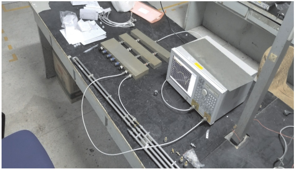
    The measured results indicate the simula-tion with one port failure right in this three-stage combiner workbench shown in Fig. 7, the VNA (Vector Network Analyzer) could gain precisely scattering parameters and phase when one port was connected with the phase shifter and the open/short terminator.

    Figure  7.  The test stand with a 360° phase shifter and mismatching components

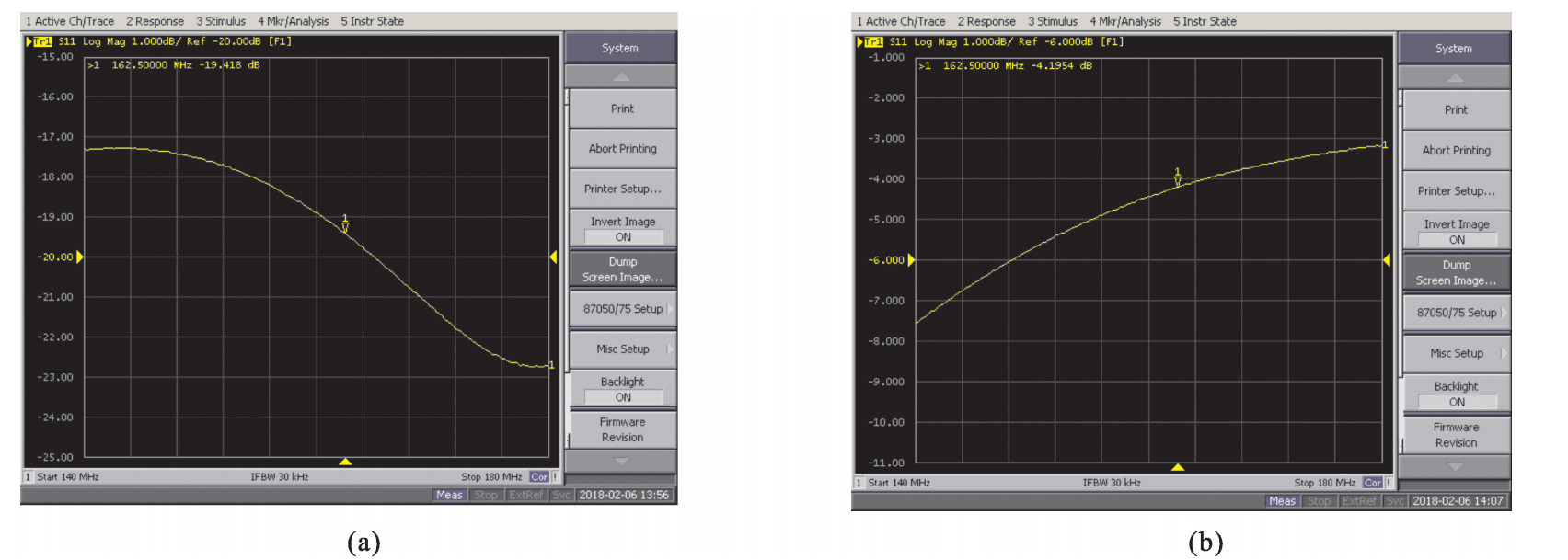
    The S parameters were measured using the workbench (Fig. 7). When only one port mismatched, the S11 excessing -20 dB indicates a very good matching (Fig. 8(a)). And in Fig. 8(b), the maximum S11 would reach up to -5 dB, which means serious mismatching when one port fails. As a result, the scattering parameter was analyzed to find out the specific regularities while the phase of the phase shifter changed gradually.

    Figure  8.  The S11 measured when one port fail

    According to the measurements, the electrical length of one phase shifter was about 118° at 162.5 MHz. Three phase shifters can cover the whole range of the S parameter, the worst matching (the block point) is shown in Fig. 9.

    Figure  9.  The worst S11 and S21 results along the full length while one port fails

    From the previous simulations and related experiments, it is obvious which of the power modules with circulator was damaged or burned down due to the severe power reflection, one reason was the unreasonable electrical length configuration between the two different levels of combiners when it is uncertain one or several ports mismatch during the operation. While the phase value meets the particular demand, the power transmission may attenuate extremely on modules, even block power completely. Thus, the very high reflected power from cavity or ports balance mismatching have a risk to accumulate on power module.

    The measurement on 8-way combiners obtained an optimum compliance to the simulation requirements. Now, five new SSAs are designed and calculated in BBEF, according to the previous experiences, the devices have shown very good characteristics of efficiency, stability, harmonics and cost, with tolerable operating risk (high risk will come from combining a large number of units). Extended versions of the module with an output power from 850 W up to 1000 W are certainly feasible on the basis of the described design concept. The next step of the development program is to study the phase relationship while any one port fails for improving reliability and reduce the risk of failure.

  • Figure  1.  The overview of BBEF 80 kW solid-state amplifier

    Figure  2.  The screenshot values when failure happened (a) and the damaged modules (b) in the amplifier

    Figure  3.  The simulated results focus on the wavelength influence from mismatch port

    Figure  4.  The simulation focused on the wavelength influence from the phase

    Figure  5.  A special three-stage combiner for the measurements during module failure

    Figure  6.  The S11 plot along different transmission line while one port is short or open-circuited

    Figure  7.  The test stand with a 360° phase shifter and mismatching components

    Figure  8.  The S11 measured when one port fail

    Figure  9.  The worst S11 and S21 results along the full length while one port fails

  • [1] Sun Liepeng, Shi Aimin, Zhang Zhouli, et al. Engineering design of the RF input couplers for C-ADS RFQ[C]//Proc of 5th International Particle Accelerator Conference. 2014: 3878-3880.
    [2] Wangler T P. Principles of RF linear accelerators[M]. New Mexico: Wiley-Interscience, 1998.
    [3] MAXIM High- Frequency/Fiber Communications Group. Single-ended and differential S-parameters. Application Note HFAN- 5.1.0(Rev. 0, 03/01)[S]. 2001.
    [4] Kurokawa K. Power waves and the scattering matrix[J]. IEEE Trans Microwave Theory Tech, 1965, 13(3): 194-202.
    [5] Xiong Zhengfeng, Ning Hui, Chen Huaibi, et al. Design of compact power combiner in rectangular waveguide[J]. High Power Laser and Particle Beams, 2014, 26: 063013. doi: 10.3788/HPLPB20142606.63013
    [6] Bockelman D E, Eisenstadt W R. Combined differential and common-mode scattering parameters: Theory and simulation[J]. IEEE Trans Microwave Theory Tech, 1995, 43(7): 1530-1539. doi: 10.1109/22.392911
    [7] Zhao Min, Zhou Xing, Wang Qingguo, et al. Design and analysis on power synthesis of all-solid-state pulse source with fast-edge[J]. High Power Laser and Particle Beams, 2015, 27: 103232. doi: 10.11884/HPLPB201527.103232
  • 加载中
图(9)
计量
  • 文章访问数:  1069
  • HTML全文浏览量:  264
  • PDF下载量:  100
  • 被引次数: 0
出版历程
  • 收稿日期:  2018-09-25
  • 修回日期:  2019-01-31
  • 刊出日期:  2019-07-15

目录

/

返回文章
返回