Study of current density distribution in terahertz device micro-electroforming process
-
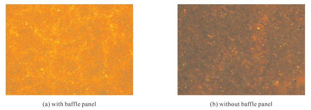
摘要: 微电铸工艺是太赫兹全金属光栅器件成型的关键工序。金属光栅质量取决于电铸工艺中金属离子沉积的均匀性, 而电铸槽阴极附近电流密度的分布直接影响金属离子沉积的均匀性。在阳极与阴极间添加开孔的绝缘玻璃挡板可以改善阴极电流密度分布的均匀性, 研究了挡板与阴极的距离以及挡板开孔大小对阴极电流密度分布的影响, 仿真结果表明: 添加开孔绝缘挡板有助于改善阴极处的电流密度分布; 当添加的玻璃挡板开孔大小与阴极尺寸一致时, 挡板距离阴极越近, 阴极的电流密度分布越均匀。根据仿真结果设计了相应的挡板, 电铸工艺获得了较好质量的均匀金属层, 从而验证了上述仿真分析的有效性。Abstract: Micro-electroforming is a key step of terahertz all-metal devices microfabrication, in which metal-ion deposit uniformity determines the grating's quality.Meanwhile, the deposit uniformity is influenced by the distribution of current density near the cathode.The current density distribution in copper micro-electroforming is investigated by method of FIT (finite integration technique) simulation analysis and experimental verification.By adding aglass baffle panel between anode and cathode, the current density uniformity can be improved.The effect of the distance between panel and cathode and the size of hole in baffle panel on current density uniformity is analyzed thoroughly.The nearer the panel is to the cathode, the more uniform the current density of the cathode, which can significantly improve the uniformity of deposit in microstructure.According to the simulation results, a baffle panel with a 2.5 cm×2.5 cm gap is fabricated and placed between the anode and the cathode with a 100 mm distance from the cathode.Then electroforming was carried out and a better quality metal layer with finer and more uniform grain was gained, which proved the simulation results.
-
Key words:
- micro-electroforming /
- terahertz /
- baffle panel /
- current density
-
表 1 各材料的电导率
Table 1. Conductivity of each material in the system of electroforming
material conductivity/(S·m-1) copper 5.8×10⁷ electroforming solution 170 SU-8 resist 10-14 baffle panel 10-14 -
[1] 刘盛纲, 钟任斌. 太赫兹科学技术及其应用的新发展[J]. 电子科技大学学报, 2009, 38(5): 481-486. doi: 10.3969/j.issn.1001-0548.2009.05.001Liu Shenggang, Zhong Renbin. Recent development of terahertz science and technology. Journal of University of Electronic Science and Technology of China, 2009, 38(5): 481-486 doi: 10.3969/j.issn.1001-0548.2009.05.001 [2] 廖复疆. 真空电子器件在100 GHz以上频段的应用[J]. 真空电子技术, 2011, (5): 50-53. doi: 10.3969/j.issn.1002-8935.2011.05.011Liao Fujiang. Vacuum electron device application at frequency above 100 GHz. Journal of Vacuum Electronics, 2011: (5): 50-53 doi: 10.3969/j.issn.1002-8935.2011.05.011 [3] 冯进军, 唐烨, 李含雁, 等. 340 GHz太赫兹反驳管振荡器[J]. 太赫兹科学与电子信息学报, 2013, 11(1): 32-37. https://www.cnki.com.cn/Article/CJFDTOTAL-XXYD201301008.htmFeng Jinjun, Tang Ye, Li Hanyan, et al. 340 GHz terahertz backward wave oscillators. Journal of Terahertz Science and Electronic Information Technology, 2013, 11(1): 32-37 https://www.cnki.com.cn/Article/CJFDTOTAL-XXYD201301008.htm [4] Li Hanyan, Li Yongtao, Feng Jinjun. Fabrication of 340-GHz folded waveguides using KMPR photoresist[J]. IEEE Electron Device Letters, 2013, 34(3): 462-464. doi: 10.1109/LED.2013.2241389 [5] Joye C D, Calame J P, Cook A M, et al. High-power copper gratings for a sheet-beam traveling-wave amplifier at G-band[J]. IEEE Trans Electrons Devices, 2013, 60(1): 506-509. doi: 10.1109/TED.2012.2226591 [6] Chen K W, Wang Y L, Chang L, et al. Investigation of overpotential and seed thickness on Damascene copper electroplating[J]. Surface & Coatings Technology, 2006, 200(10): 3112-3116. [7] Yang H, Kang S W. Improvement of thickness uniformity in nickel electro-forming for the LIGA process[J]. International Journal of Machine Tools &Manufacture, 2000, 40(7): 1065-1072. [8] 李国锋, 王翔, 何冀军, 等. 微细电铸电流密度的有限元分析[J]. 微细加工技术, 2007(6): 35-38. https://www.cnki.com.cn/Article/CJFDTOTAL-WXJS200706010.htmLi Guofeng, Wang Xiang, He Jijun, et al. Finite element analysis of the current density distribution in micro-electroforming. Micro-Fabrication Technology, 2007(6): 35-38 https://www.cnki.com.cn/Article/CJFDTOTAL-WXJS200706010.htm [9] 汤俊, 汪红, 刘瑞, 等. MEMS微结构电沉积层均匀性的有限元模拟[J]. 微细加工技术, 2008(5): 45-49. https://www.cnki.com.cn/Article/CJFDTOTAL-WXJS200805016.htmTang Jun, Wang Hong, Liu Rui, et al. FEM simulation of the uniformity of the thickness of the MEMS microstructure electro-deposition. Micro-Fabrication Technology, 2008(5): 45-49 https://www.cnki.com.cn/Article/CJFDTOTAL-WXJS200805016.htm [10] 刘太权. 电镀层均匀性的数值模拟及验证[J]. 电镀与环保, 2010, 30(2): 11-13. doi: 10.3969/j.issn.1000-4742.2010.02.004Liu Taiquan. Numerical simulation and verification on the uniformity of electroplated coating. Electroplating & Pollution Control, 2010, 30(2): 11-13 doi: 10.3969/j.issn.1000-4742.2010.02.004 [11] 王星星, 雷卫宁, 刘维桥, 等. MEMS微器件电沉积层均匀性的研究进展[J]. 稀有金属材料与工程, 2011, 40(12): 2245-2251. https://www.cnki.com.cn/Article/CJFDTOTAL-COSE201112039.htmWang Xingxing, Lei Weining, Liu Weiqiao, et al. Research progress on uniformity of MEMS micro-device electro-deposition. Rare metal materials and engineering, 2011, 40(12): 2245-2251 https://www.cnki.com.cn/Article/CJFDTOTAL-COSE201112039.htm [12] 董久超, 王磊, 汤俊, 等. 电镀层均匀性的Ansys模拟与优化[J]. 新技术新工艺, 2008(11): 114-117. doi: 10.3969/j.issn.1003-5311.2008.11.041Dong Jiuchao, Wang Lei, Tang Jun, et al. Ansys simulation and optimization of electro coating uniformity. New Techniques and Technology, 2008(11): 114-117 doi: 10.3969/j.issn.1003-5311.2008.11.041 [13] 蔡元兴, 孙齐磊. 电镀电化学原理[M]. 北京: 化学工业出版社. 2014: 4-5.Cai Yuanxing, Sun Qilei. Electrochemical principle. Beijing. Chemical Industry Press, 2014: 4-5 -


 下载:
下载:


