

Microwave damage susceptibilitytrend of the silicon NPN monolithic composite transistor as a function of structure parameters
-
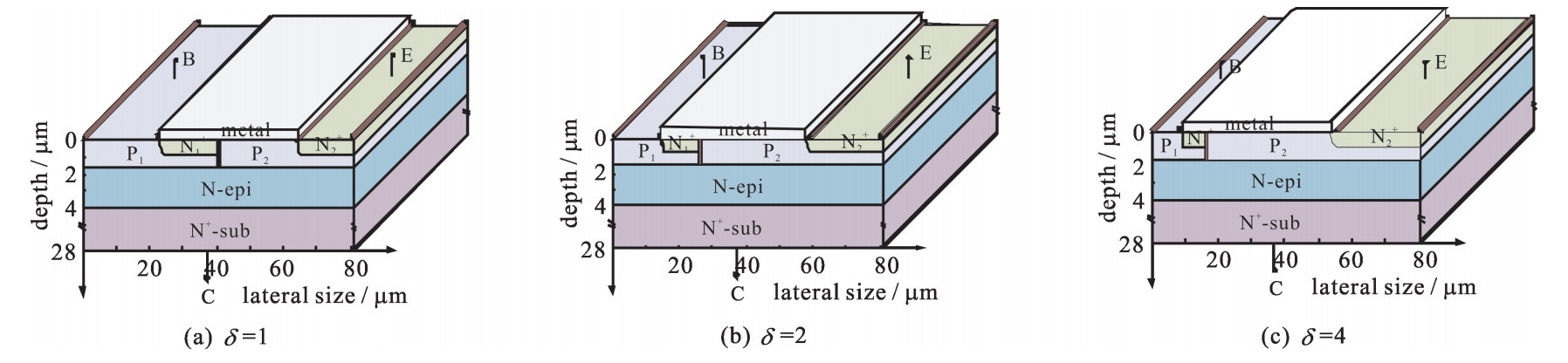
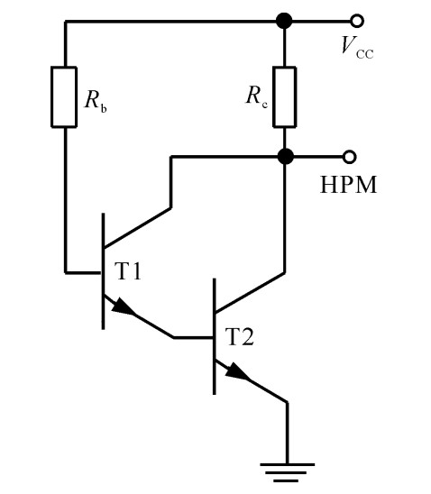
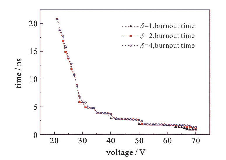
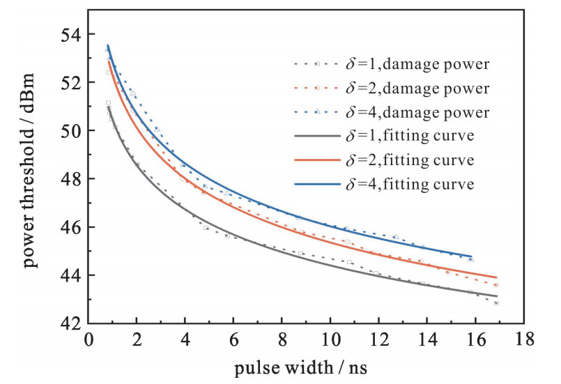
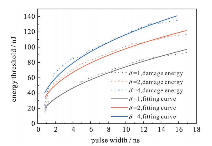
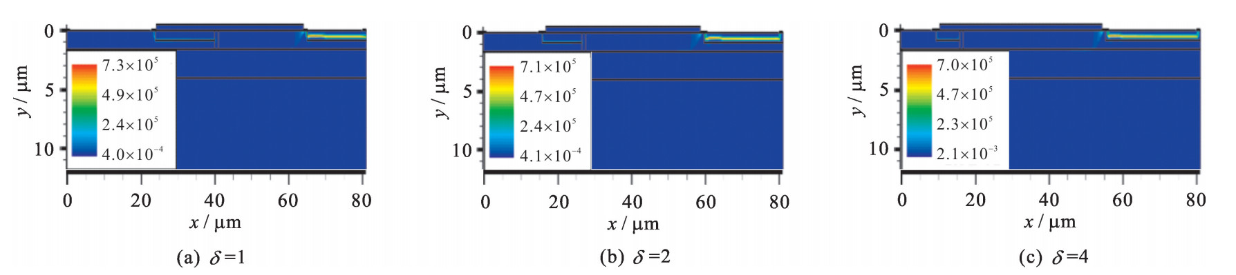
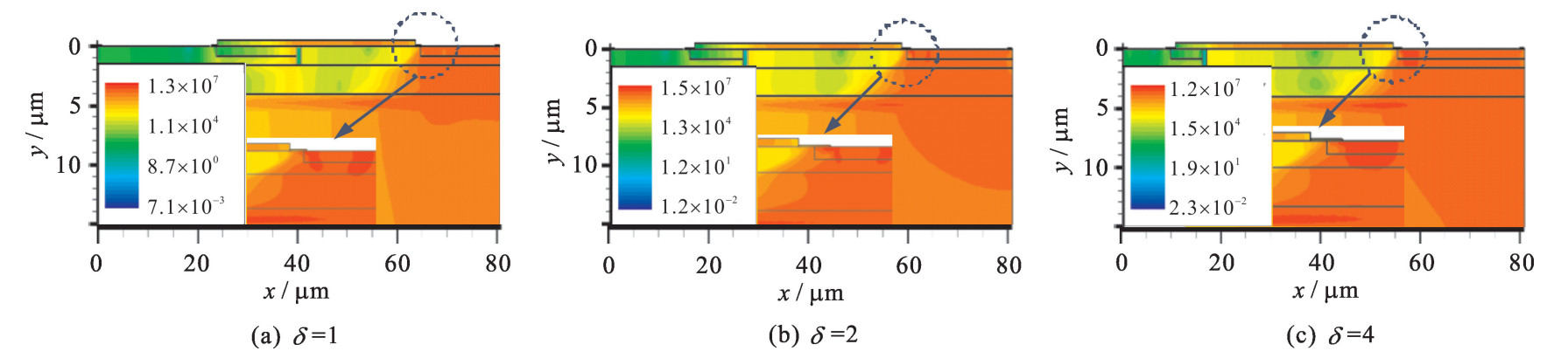
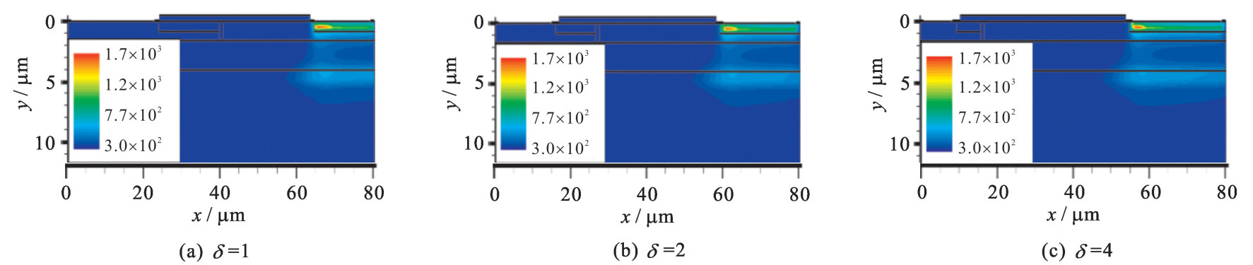
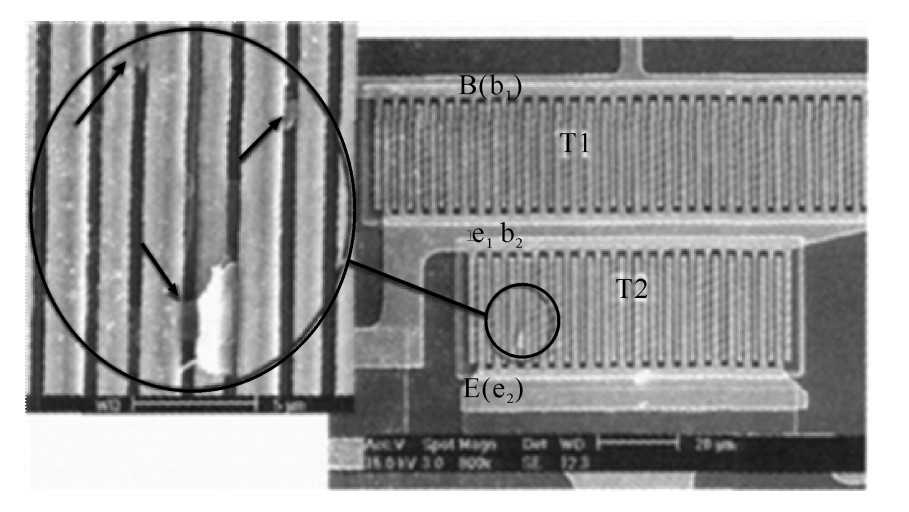
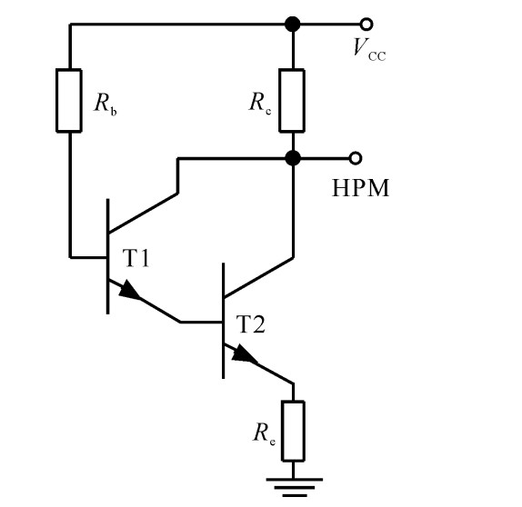
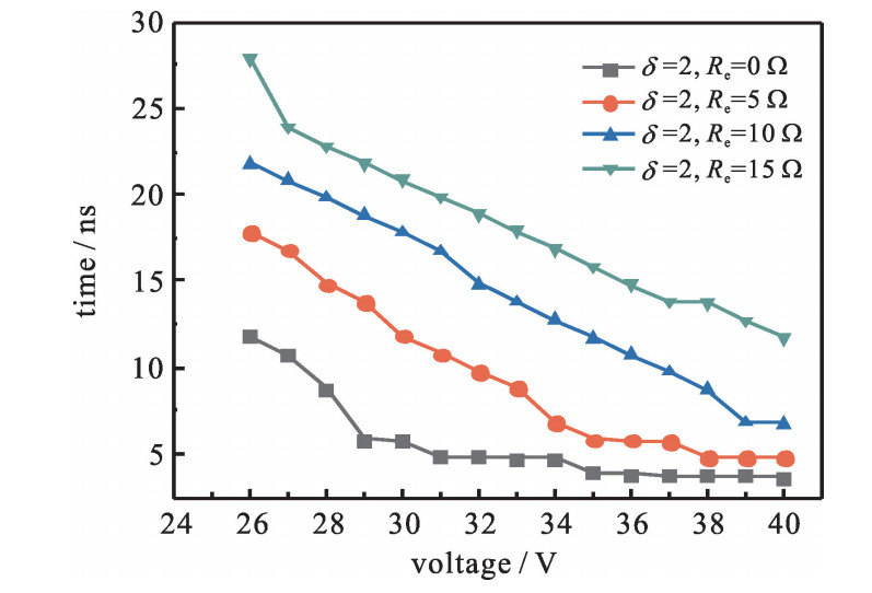
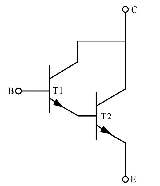
摘要: 建立了三种不同结构的硅基单片式复合晶体管(由T1和T2两个晶体管构成)的二维电热模型,研究了高功率微波对不同结构的硅基单片式复合晶体管的损伤效应的影响。获得了不同器件结构下导致复合晶体管损伤的损伤功率阈值和损伤能量阈值分别与脉宽的关系。结果表明,当复合晶体管的总体尺寸不变而T2和T1晶体管的面积比值更大时需要更多的功率和能量来损伤器件。通过分析器件内部电场、电流密度和温度分布的变化,得到了复合晶体管的结构对其微波损伤效应的影响规律。对比发现,三种结构的复合晶体管的损伤点均位于T2管的发射极附近,随着T2和T1晶体管面积比的增大,电场、电流密度和温度在器件内部的分布将变得更加分散。此外,在发射极处增加外接电阻Re,研究表明损伤时间随发射极电阻的增大而增加。因此可以得出结论,适当改变器件结构或增加外接元件可以增强器件的抗微波损伤能力。晶体管的仿真毁伤点与实验结果一致。Abstract: This paper presents a theoretical study on the influences of the device structure parameters on the damage progress of the silicon NPN monolithic composite transistor induced by injection power. The silicon NPN monolithic composite transistors (composed by two successive transistors, T1 and T2) with three different structural parameters are established utilizing the circuit simulator, Sentaurus-TCAD. The dependences of the damage energy threshold and the damage power threshold required to cause the device failure on the pulse-width are obtained. The results show that higher power threshold and more energy are needed to damage the device if the area of the T2 transistor is larger. A study of the damage mechanism is conducted based on the variation analysis of the distributions of the electric field, current density, and temperature in the device. It is found that the distributions of the electric field, current density, and temperature become more dispersed as the area of the T2 transistor increases. It is concluded that when the overall area of the silicon NPN monolithic composite transistor is constant, and as the area ratio of the T2 transistor and the T1 transistor increases, the device becomes less vulnerable to damage. Moreover, the emitter resistor Re has a significant effect on the burnout time. The simulated burnt spot position of the transistor is in good agreement with the experimental result.
-
[1] Kim K, Iliadis A A. Latch-up effects in CMOS inverters due to high power pulsed electromagnetic interference[J]. Solid-State Electronics, 2008, 52(10): 1589-1593. doi: 10.1016/j.sse.2008.06.041 [2] Kim K, Iliadis A A. Operational upsets and critical new bit errors in CMOS digital inverters due to high power pulsed electromagnetic interference[J]. Solid-State Electronics, 2010, 54(1): 18-21. doi: 10.1016/j.sse.2009.09.006 [3] Korte S, Camp M, Garbe H. Hardware and software simulation of transient pulse impact on integrated circuits[C]//2005 International Symposium on Electromagnetic Compatibility. 2005, 2: 489-494. [4] Liu Yang, Chai Changchun, Yang Yintang, et al. Damage effect and mechanism of the GaAs high electron mobility transistor induced by high power microwave[J]. Chinese Physics B, 2016, 25(4): 465-470. [5] Chen Jie, Du Zhengwei. Device simulation studies on latch-up effects in CMOS inverters induced by microwave pulse[J]. Microelectronics Reliability, 2013, 53(3): 371-378. doi: 10.1016/j.microrel.2012.10.012 [6] Chen Jie, Du Zhengwei. Understanding and modeling of internal transient latch-up susceptibility in CMOS inverters due to microwave pulses[J]. Microelectronics Reliability, 2013, 53(12): 1891-1896. doi: 10.1016/j.microrel.2013.07.004 [7] Backstrom M G, Lovstrand K G. Susceptibility of electronic systems to high-power microwaves: Summary of test experience[J]. IEEE Trans Electromag Compat, 2004, 46(3): 396-403. doi: 10.1109/TEMC.2004.831814 [8] Kim K, Iliadis A A. Operational upsets and critical new bit errors in CMOS digital inverters due to high power pulsed electromagnetic interference[J]. Solid State Electronics, 2009, 54(1): 18-21. [9] Ma Zhenyang, Chai Changchun, Ren Xingrong, et al. The damage effect and mechanism of the bipolar transistor caused by microwaves[J]. Acta Physica Sinica, 2012, 61(7): 511-517. [10] Ma Zhenyang, Chai Changchun, Ren Xingrong, et al. Effects of microwave pulse-width damage on a bipolar transistor[J]. Chinese Physics B, 2012, 21(5): 679-684. [11] Zhou Huaian, Du Zhengwei, Gong Ke. Transient response of bipolar junction transistor under intense electromagnetic pulse[J]. High Power Laser and Particle Beams, 2005, 17(12): 1861-1864. [12] Ma Zhenyang, Chai Changchun, Ren Xingrong, et al. The pulsed microwave damage trend of a bipolar transistor as a function of pulse parameters[J]. Chinese Physics B, 2013, 22(2): 538-542. [13] Ma Zhenyang, Chai Changchun, Ren Xingrong, et al. Microwave damage susceptibility trend of a bipolar transistor as a function of frequency[J]. Chinese Physics B, 2012, 21(9): 565-570. [14] Ghandi R, Buono B, Domeij M, et al. High current-gain implantation-free 4H-SIC monolithic Darlington transistor[J]. IEEE Electron Device Letters, 2011, 32(2): 188-190. [15] Zhang Qingchun, Jonas C, O'Loughlin M, et al. A 10-kV monolithic Darlington transistor with β of 336 in 4H-SiC[J]. IEEE Electron Device Letters, 2009, 30(2): 142-144. [16] Kumar M J, Sharma A. New silicon carbide(SiC) hetero-junction Darlington transistor[C]//2006 Annual IEEE India Conference. 2006. [17] Tang Y, Chow T P. Monolithic 4H-SIC Darlington transistor with a peak current gain of 2000[C]//61st Device Research Conference. 2003. [18] Lu Yashi, Zhang Wei, Liu Zhihong, et al. A Darlington SiGe microwave monolithic integrated circuit[C]//2006 IEEE Mediterranean Electrotechnical Conference. 2006. [19] Chai Changchun, Yang Yintang, Zhang Bing, et al. Mechanism of energy-injection damage of silicon bipolar low-noise amplifiers[J]. J Semicond, 2008(12): 2403-2407. [20] Li Hui, Chai Changchun, Yang Yintang, et al. Damage effects and mechanism of the silicon NPN monolithic composite transistor induced by high-power microwaves[J]. Chinese Physics B, 2018, 27(8): 637-643. [21] Wang Qiankun, Chai Changchun, Yang Yintang, et al. The influence of pulsed parameters on the damage of a Darlington transistor[J]. Journal of Semiconductors, 2018, 39(9): 2-47. [22] Korte S, Camp M, Garbe, H. Hardware and software simulation of transient pulse impact on integrated circuits[C]//IEEE International Symposium on Electromagnetic Compatibility. 2005. [23] Wunsch D C, Bell R R. Determination of threshold failure levels of semiconductor diodes and transistors due to pulse voltages[J]. IEEE Trans Nuclear Science, 1968, 15(6): 244-259. [24] Tasca D M. Pulse power failure modes in semiconductors[J]. IEEE Trans Nuclear Science, 1970, 17(6): 364-372. -

 下载:
下载:

 点击查看大图
图(13)
计量
- 文章访问数: 1275
- HTML全文浏览量: 327
- PDF下载量: 47
- 被引次数: 0
