留言板

尊敬的读者、作者、审稿人, 关于本刊的投稿、审稿、编辑和出版的任何问题, 您可以本页添加留言。我们将尽快给您答复。谢谢您的支持!

姓名
邮箱
手机号码
标题
留言内容
验证码

GaAs-PCSS多通道同步导通条件实验研究

刘毅 谌怡 夏连胜 王卫 叶茂 张篁

刘毅, 谌怡, 夏连胜, 等. GaAs-PCSS多通道同步导通条件实验研究[J]. 强激光与粒子束, 2020, 32: 025005. doi: 10.11884/HPLPB202032.190328
引用本文: 刘毅, 谌怡, 夏连胜, 等. GaAs-PCSS多通道同步导通条件实验研究[J]. 强激光与粒子束, 2020, 32: 025005. doi: 10.11884/HPLPB202032.190328
Liu Yi, Shen Yi, Xia Liansheng, et al. Experimental study on multi-channel synchronous conduction conditions of GaAs-PCSS[J]. High Power Laser and Particle Beams, 2020, 32: 025005. doi: 10.11884/HPLPB202032.190328
Citation: Liu Yi, Shen Yi, Xia Liansheng, et al. Experimental study on multi-channel synchronous conduction conditions of GaAs-PCSS[J]. High Power Laser and Particle Beams, 2020, 32: 025005. doi: 10.11884/HPLPB202032.190328

GaAs-PCSS多通道同步导通条件实验研究

doi: 10.11884/HPLPB202032.190328
基金项目: 国家自然科学基金项目(51507162,51407169,51607166);国家自然科学基金委员会与中国工程物理研究院联合基金项目(U1530156)
详细信息
    作者简介:

    刘 毅(1987-),男,硕士,助理研究员,从事脉冲功率技术及加速器技术研究;109854434@163.com

  • 中图分类号: TM834

Experimental study on multi-channel synchronous conduction conditions of GaAs-PCSS

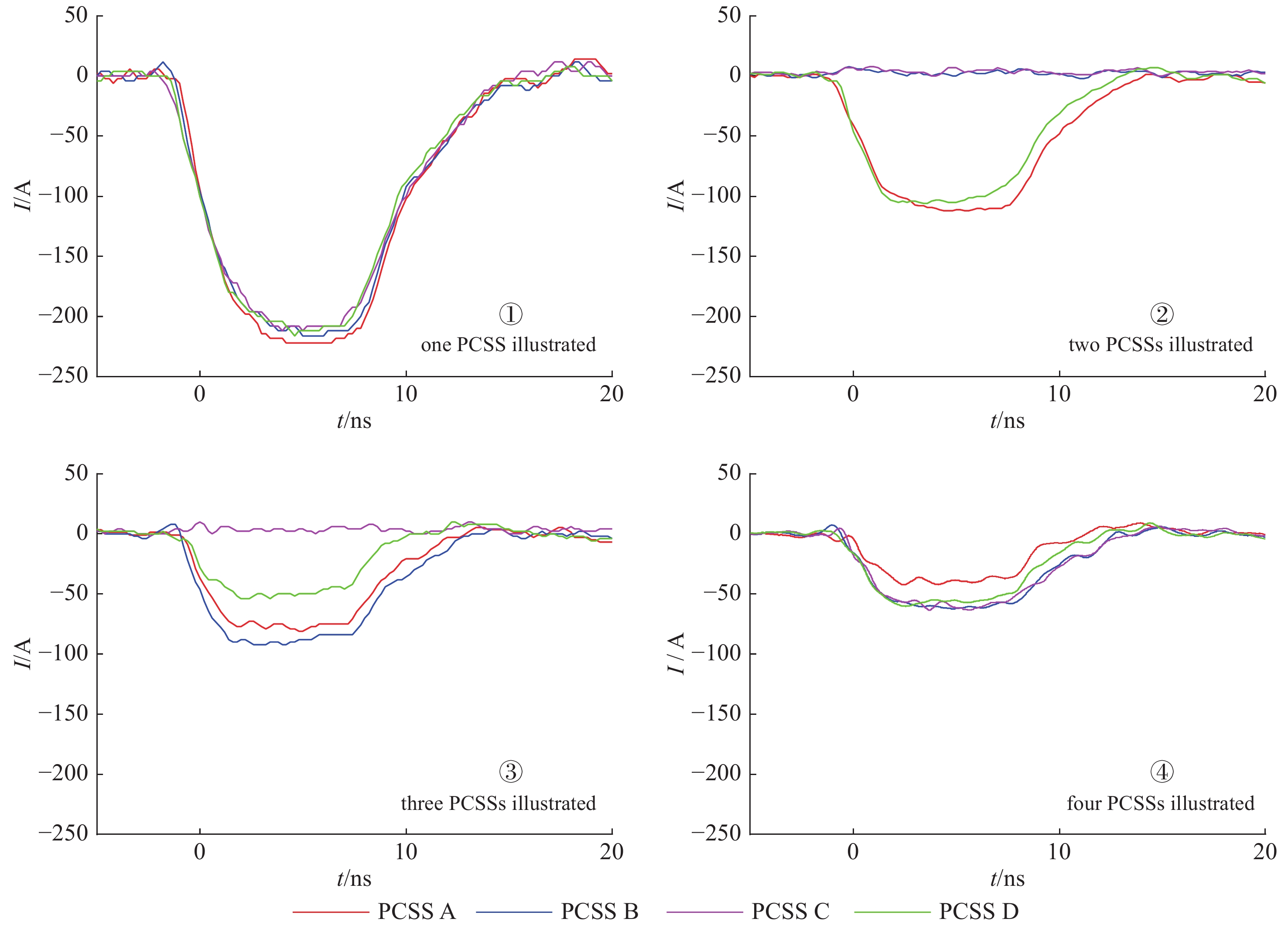
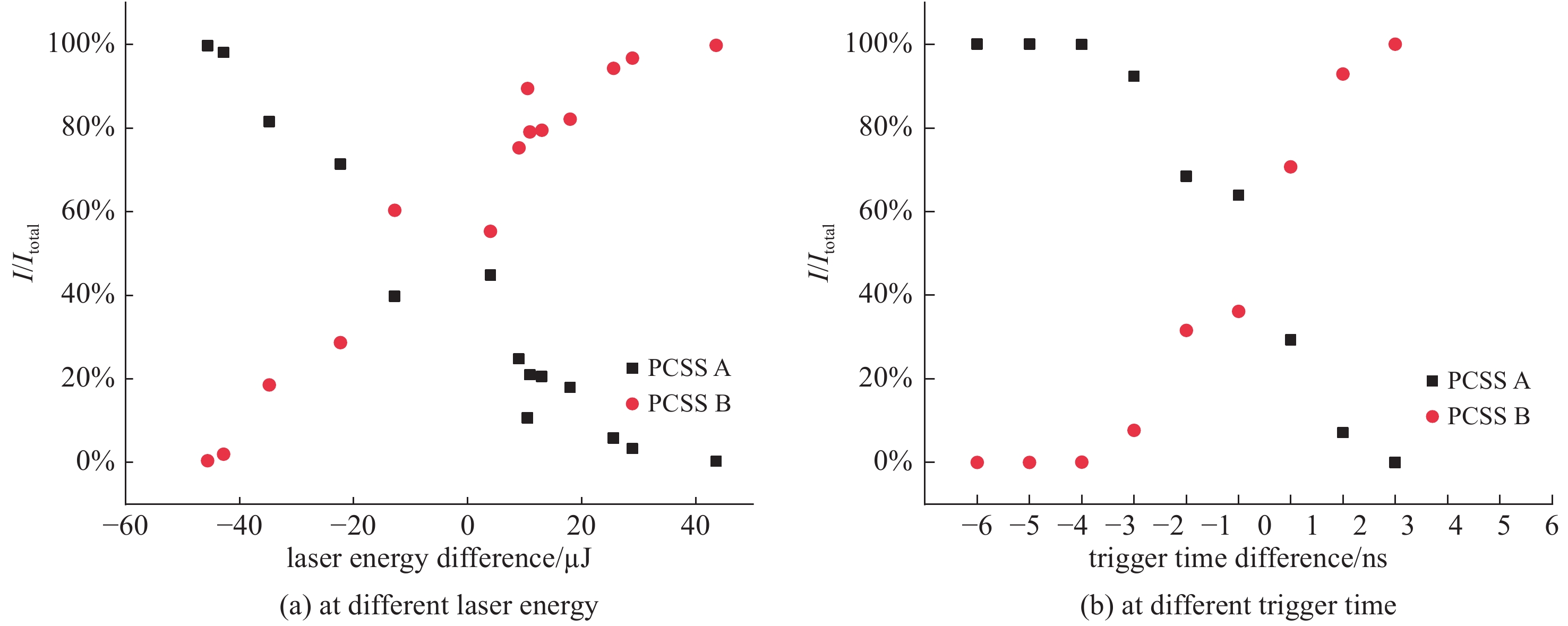
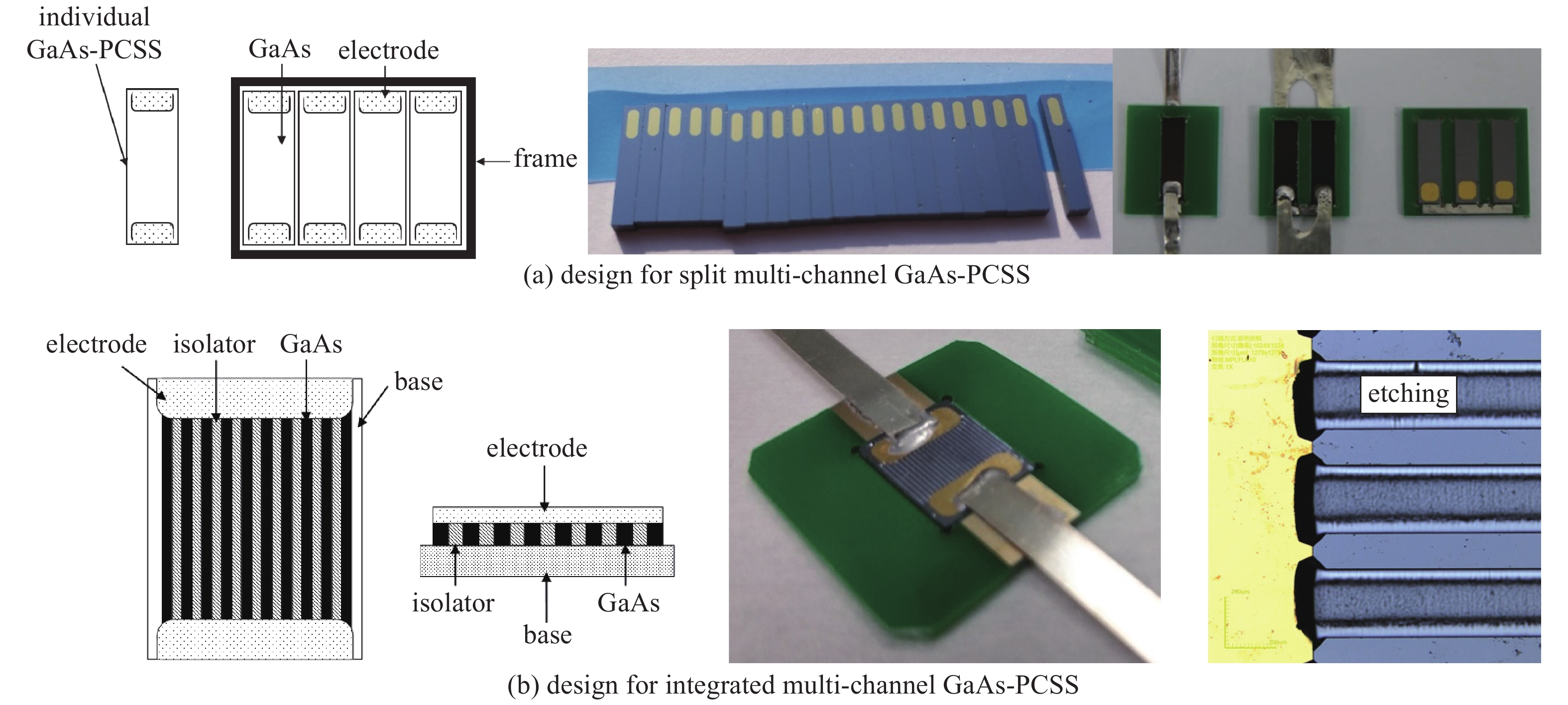
  • 摘要: 砷化镓光导开关(GaAs-PCSS)是具有快响应、高重频、低抖动、高功率容量的半导体光电导开关,多通道设计能够有效降低GaAs-PCSS非线性大电流导通时的损伤,提高开关寿命。为探究GaAs-PCSS多通道同步导通的必要条件,在基于固态脉冲形成线的实验平台上,通过特殊设计的夹具,将多枚GaAs-PCSS并联连接以作为脉冲形成电路的开关,以对各GaAs-PCSS施以不同的触发信号进行测试。实验结果证明:相同触发信号下,开关导通电流被成功地均分到4个GaAs-PCSS通道中;不同触发信号下,为获得较好的电流均分效果,各通道触发延迟时差须小于1 ns,触发能量差须小于20 μJ。设计了分体式、单体式两种结构的多通道GaAs-PCSS,其中基于刻蚀工艺的单体式20通道GaAs-PCSS在7 000余次大电流工作后仅发生轻微损伤。
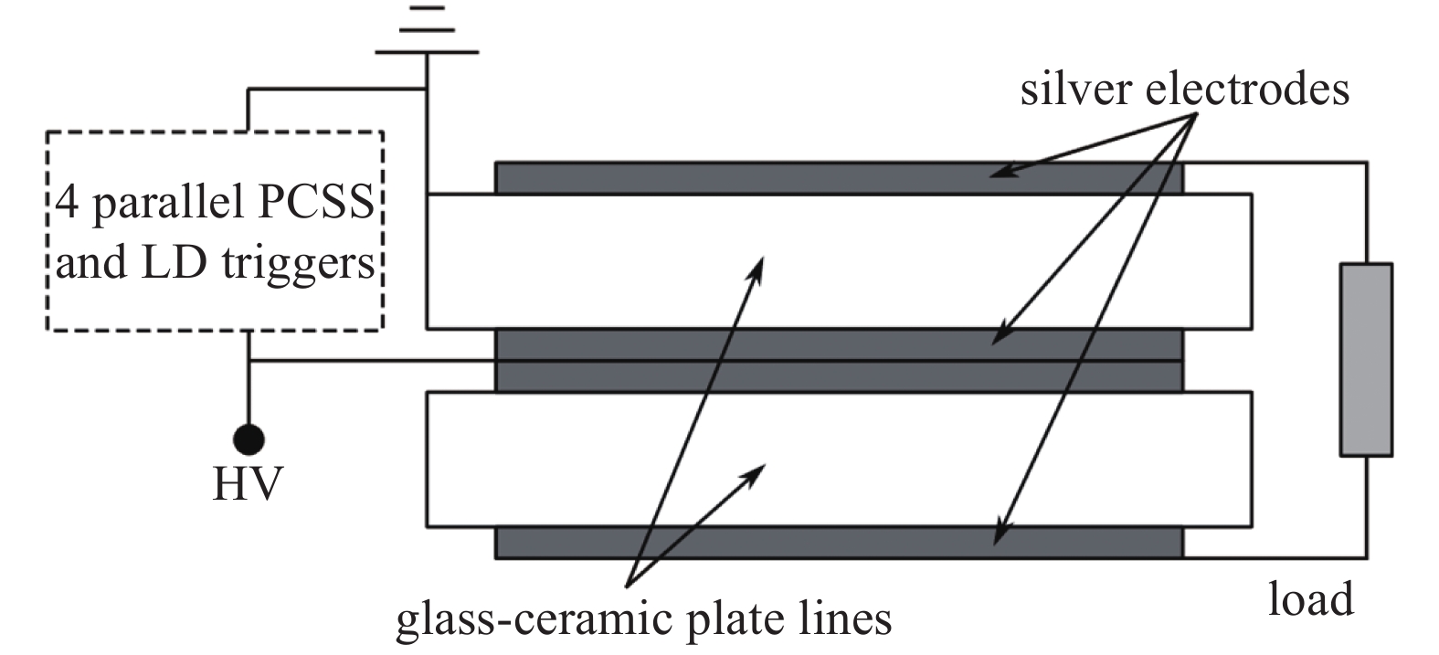
  • 图  1  实验平台电路示意图

    Figure  1.  Schematic of experimental circuit

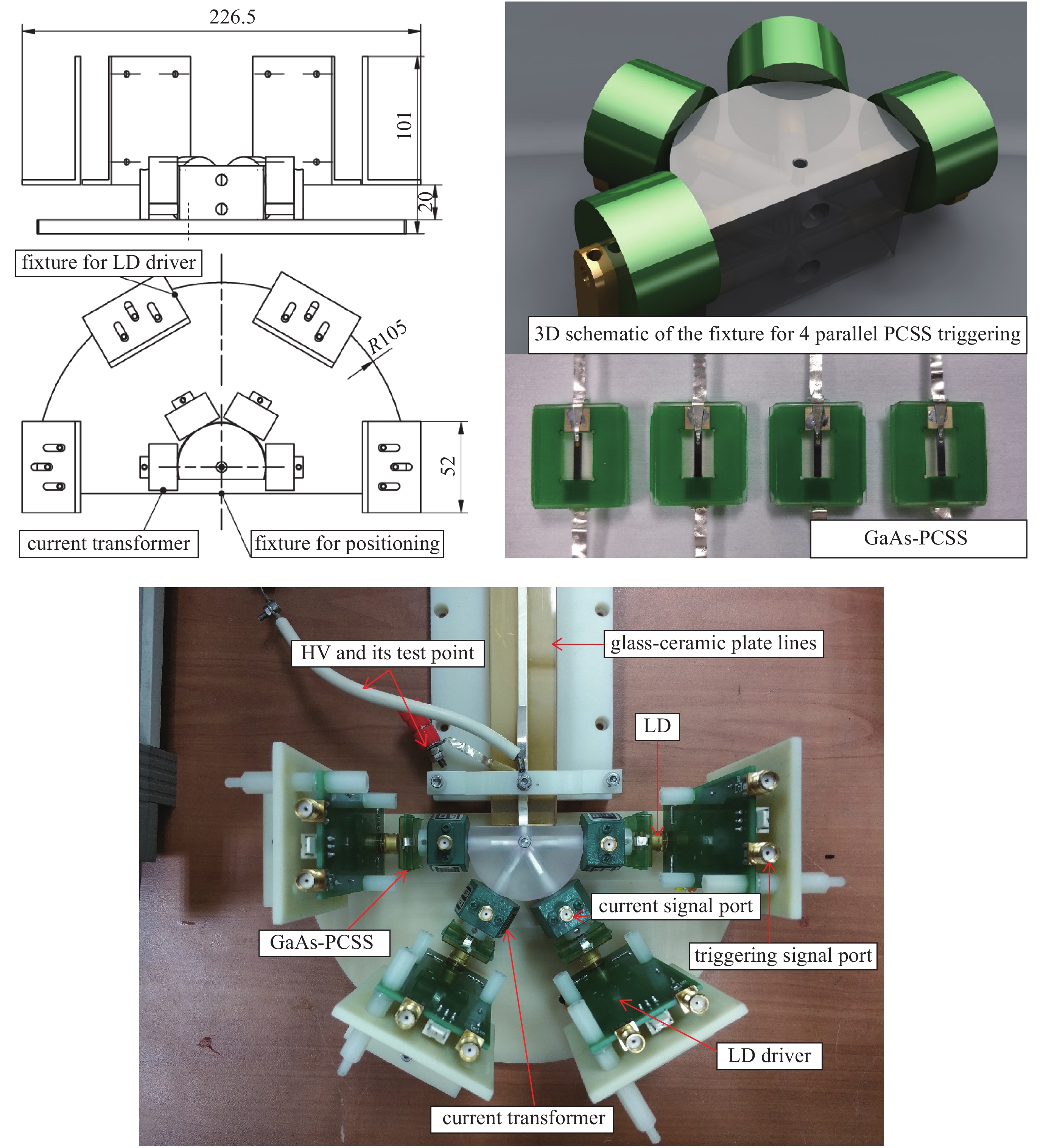
    图  2  四GaAs-PCSS并联同步导通触发与测试平台

    Figure  2.  Experimental platform for 4 parallel GaAs-PCSS triggering test

    图  3  各开关中导通电流测试结果

    Figure  3.  Conducting current of each PCSS when 1, 2, 3 or 4 PCSSs are triggered

    图  4  各开关中导通电流百分比与触发能量或触发延迟时间差之间的关系

    Figure  4.  Percentage of conducting current of each PCSS when triggered at different laser energy or trigger time

    图  5  分体式和单体式多通道GaAs-PCSS设计与照片

    Figure  5.  Designs and pictures of split and integrated multi-channel GaAs-PCSS

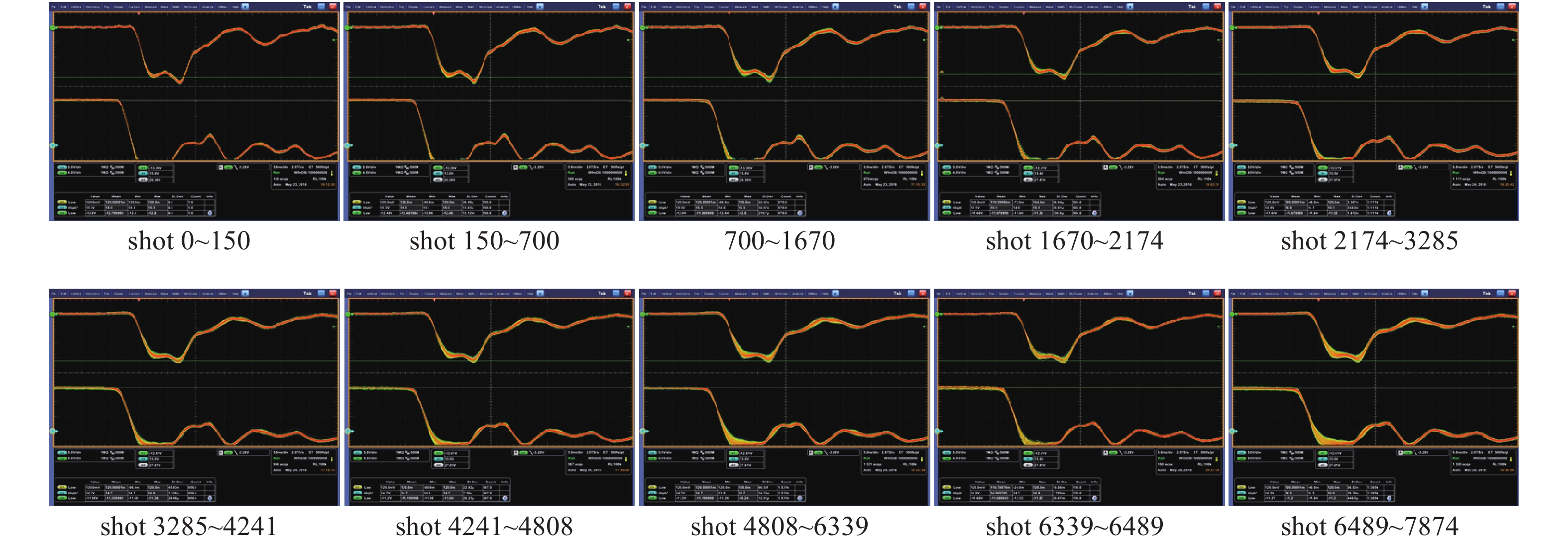
    图  6  单体式20通道GaAs-PCSS的7 000余次导通波形累积图

    Figure  6.  Cumulative graph of load output waveforms (up) and bias voltage (down) of the integrated multi-channel GaAs-PCSS during 7 000 shots

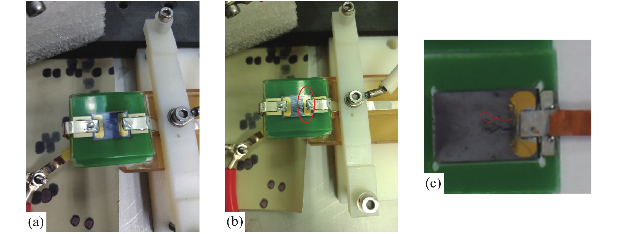
    图  7  单体式20通道GaAs-PCSS的7 000余次导通前(a)、后(b)对比照,及普通GaAs-PCSS损伤照片(c)

    Figure  7.  Photos of the integrated 20-channel GaAs-PCSS before (a) and after (b) 7 000 shots, and a photo of a damaged normal GaAs-PCSS (c)

  • [1] Loubriel G M, Zutavern F J, Baca A G, et al. Photoconductive semiconductor switches[J]. IEEE Trans Plasma Sci, 1997, 25(2): 124-130. doi: 10.1109/27.602482
    [2] Shi W, Tian L, Liu Z, et al. Accurate measurement of the jitter time of GaAs photoconductive semiconductor switches triggered by a one-to-two optical fiber[J]. Appl Phys Lett, 2013, 102: 154106. doi: 10.1063/1.4802755
    [3] Yuan Jianqiang, Xie Weiping, Zhou Liangji, et al. Developments and applications of photoconductive semiconductor switches in pulsed power technology[J]. High Power Laser and Particle Beams, 2008, 20(1): 171-176.
    [4] Nunally W C. Critical component requirements for compact pulse power system architectures[J]. IEEE Trans Plasma Sci, 2005, 33(4): 1262-1267. doi: 10.1109/TPS.2005.852406
    [5] Schoenberg J S H, Burger J W, Tyo J S, et al. Ultra-wideband source using gallium arsenide photoconductive semiconductor switches[J]. IEEE Trans Plasma Sci, 1997, 25(2): 327-334. doi: 10.1109/27.602507
    [6] Nunally W C. High-power microwave generation using optically activated semiconductor switches[J]. IEEE Trans Electron Devices, 1990, 37(12): 2439-2448. doi: 10.1109/16.64516
    [7] Liu Yi, Wang Wei, Shen Yi, et al. Lifetime of high-power GaAs photoconductive semiconductor switch triggered by laser of different power density[C]// Proc of SPIE. 2014: 92554G.
    [8] 施卫, 田立强. 半绝缘GaAs光电导开关的击穿特性[J]. 半导体学报, 2004, 25(6):691-696. (Shi Wei, Tian Liqiang. Breakdown characteristics of semi-insulating GaAs photoconductive switch[J]. Journal of Semiconductors, 2004, 25(6): 691-696 doi: 10.3321/j.issn:0253-4177.2004.06.015
    [9] Loubriel G M, Zutavern F J, Mar A, et al. Longevity of optically activated, high gain GaAs photoconductive semiconductor switches[J]. IEEE Trans Plasma Science, 1998, 26(5): 1393-1402. doi: 10.1109/27.736024
    [10] 杨宏春, 崔海娟, 孙云卿, 等. 高功率、长寿命GaAs光电导开关[J]. 科学通报, 2010, 55(13):1331-1337. (Yang Hongchun, Cui Haijuan, Sun Yunqin, et al. High power, longevity gallium arsenide photoconductive semiconductor switches[J]. Chinese Sci Bull, 2010, 55(13): 1331-1337
    [11] Saiz T A, Zutavern F J, Glover S F, et al. PCSS lifetime testing for pulsed power applications[C]//Proc of 16th IEEE International Conference on Pulsed Power. 2007: 106-109.
    [12] Zutavern F J, Mar A, Vawter G A, et al. Multi-filament PCSS modules to replace high current pulsed power switches[C]//Proc of 19th IEEE International Conference on Pulsed Power. 2013: 1-6.
  • 加载中
图(7)
计量
  • 文章访问数:  1437
  • HTML全文浏览量:  547
  • PDF下载量:  82
  • 被引次数: 0
出版历程
  • 收稿日期:  2019-09-02
  • 修回日期:  2019-10-12
  • 刊出日期:  2019-12-26

目录

    /

    返回文章
    返回