Influence of nitrogen ion implantation on surface charge accumulation and dissipation of polytetrafluoroethylene
-
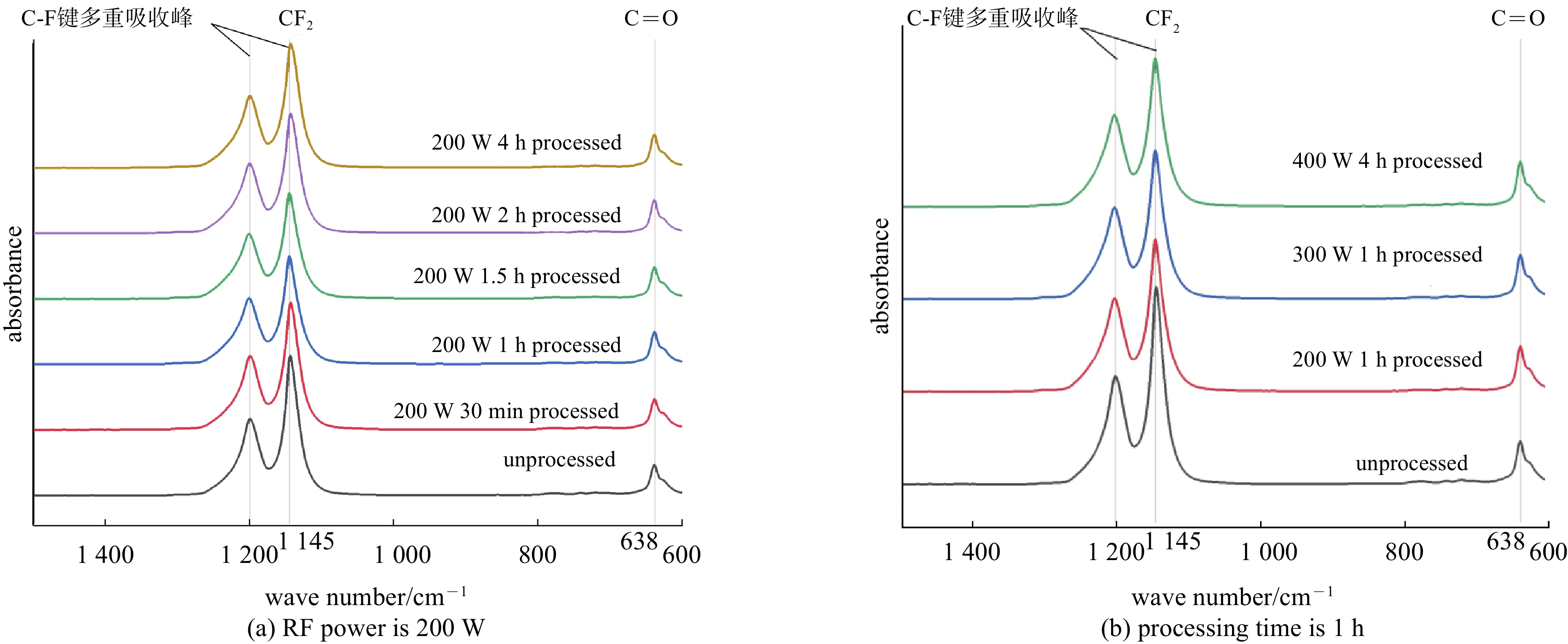
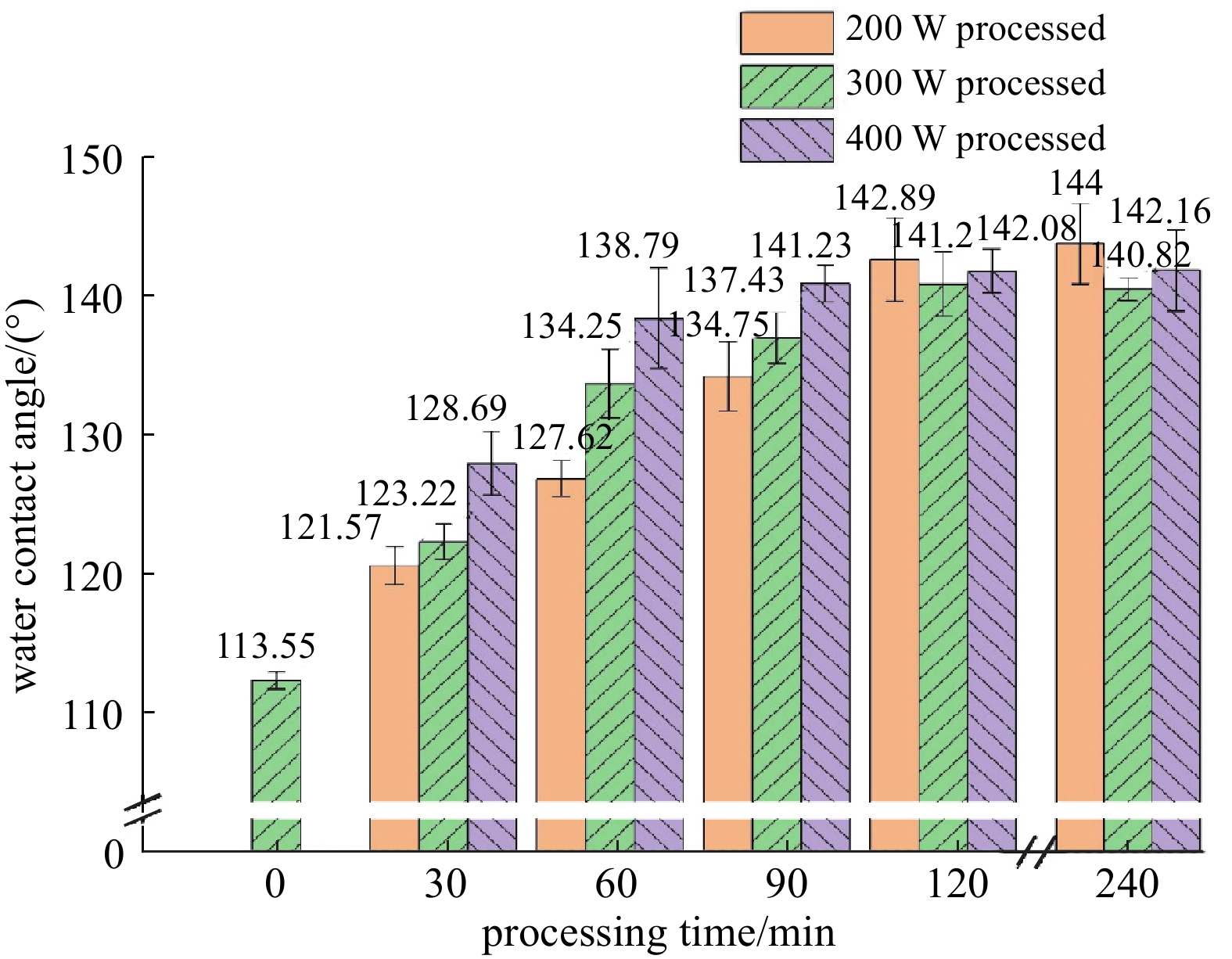
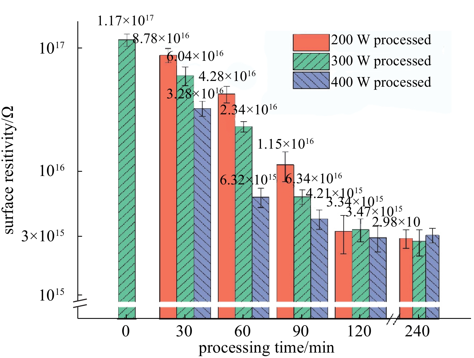
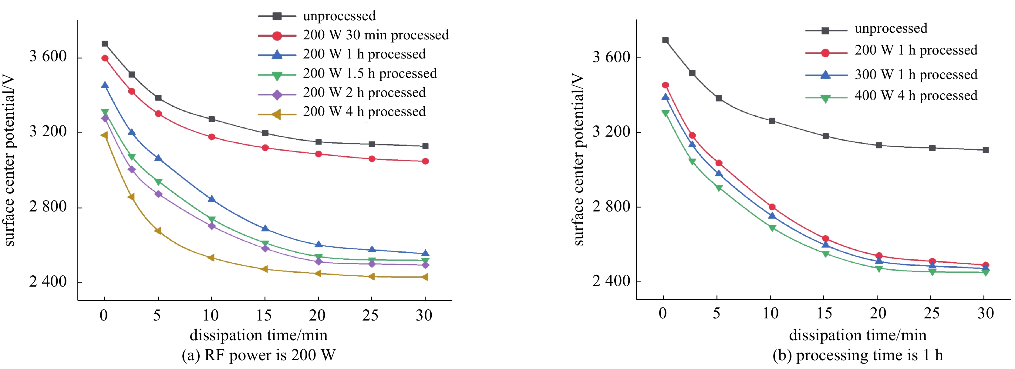
摘要: 为了抑制聚四氟乙烯材料表面电荷积聚,采用射频产生氮等离子体对其表面进行等离子体浸没离子注入以改善其表面性能。对注入前后的聚四氟乙烯材料样品进行了X射线光电子能谱分析(XPS)、傅里叶红外光谱测试(FTIR)、水接触角测量、表面电阻率测量以及表面电位衰减测量,并基于等温表面电位衰减理论对其表面陷阱能级和密度分布进行了计算,以分析聚四氟乙烯样品经离子注入处理后其表面成分和物理性能的变化,并研究了这些变化对聚四氟乙烯样品表面电荷积聚和消散特性的影响。结果表明:氮离子注入后,聚四氟乙烯材料表面化学成分的主要变化是自身分子结构的破坏和转化,部分CF2结构转变为CF和CF3结构,导致样品表面陷阱能级变浅;水接触角升至140°左右,比未处理样品上升了约27°,表面电阻率降至3×10¹⁵ Ω,比未处理样品下降了两个数量级;表面电晕放电1 min后,经氮离子注入处理的聚四氟乙烯材料表面积聚电荷量减少,消散速度加快,这是因为表面陷阱能级变浅有利于表面电荷脱陷,同时表面电阻率降低也促进了表面电荷沿面传导的消散过程,聚四氟乙烯样品表面陷阱能级分布曲线也证实了这一论点。Abstract: To suppress the accumulation of charge on the surface of polytetrafluoroethylene (PTFE) material, radio frequency nitrogen plasma was generated to perform plasma immersion ion implantation (PIII) on the PTFE surface to improve its surface properties. X-ray photoelectron spectroscopy (XPS), Fourier transform infrared spectroscopy (FTIR), water contact angle measurement, surface resistivity measurement and surface potential attenuation measurement were performed on the samples of PTFE material before and after injection to analyze the changes in surface composition and physical properties of PTFE samples after ion implantation treatment. Based on the theory of isothermal surface potential attenuation, the energy levels and density distributions of the surface traps were calculated. The results show that after nitrogen ion implantation, the main change in the chemical composition of the surface of the PTFE material is the destruction and conversion of its own molecular structure, and part of the CF2 structure is transformed into the CF and CF3 structures, resulting in shallower trap levels on the sample surface. The results also show that the water contact angle rose to about 140°, which is about 27° higher than that of the unprocessed sample. The surface resistivity drops to 3×10¹⁵ Ω, which is two orders of magnitude lower than that of the unprocessed samples. After 1 min of corona discharge on the surface, the amount of accumulated charge on the surface of the PTFE material processed with nitrogen ion implantation decreased, and the rate of dissipation increased. This is because the lower surface trap level is conducive to surface charge trapping, and the reduction in surface resistivity also promotes the dissipation process of surface charge along the surface. The curve of trap level distribution on the surface of PTFE sample also confirmed this.
-
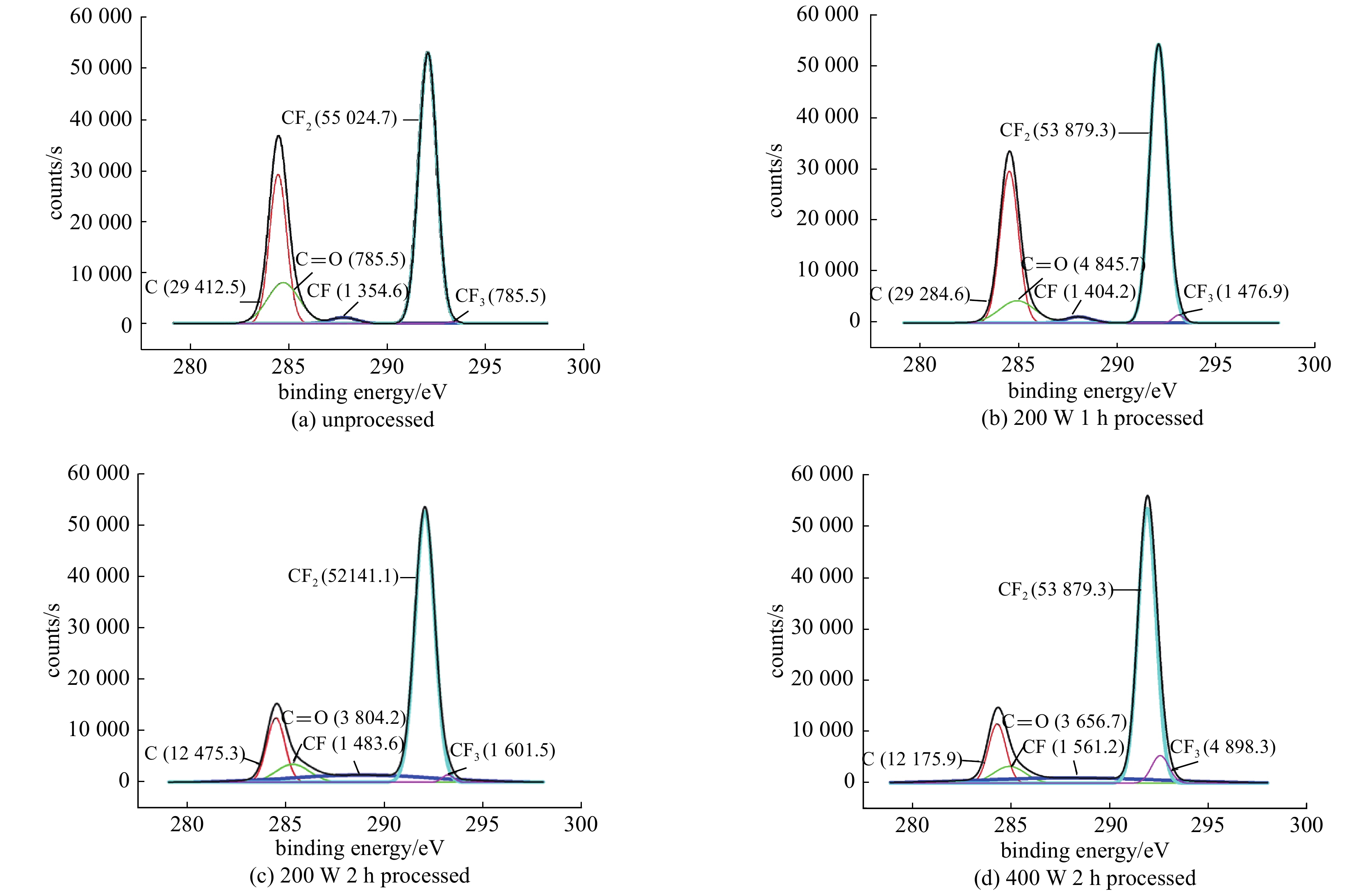
表 1 离子注入处理前后PTFE样品表面C元素各状态含量比例
Table 1. Proportion of content of element C in PTFE sample surface before and after ion implantation
RF power/W processing time/h proportion/% C C=O CF CF2 CF3 0 0 31.1 8.4 1.4 58.2 0.8 200 1 32.2 5.3 1.5 59.5 1.6 200 2 17.4 5.3 2.1 72.9 2.2 400 2 16.6 5.0 2.1 69.5 6.7 表 2 不同射频功率和处理时间下的PTFE样品表面陷阱能级和密度
Table 2. Energy level and density of traps on the surface of PTFE samples under different RF power and processing time
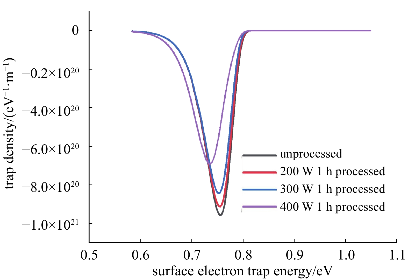
RF power/W processing time/h surface trap level/eV surface trap density/(1020 eV−1·m−3) 0 0 0.756 9.82 200 1 0.754 9.19 200 2 0.755 8.56 400 2 0.735 7.04 -
[1] 谢苏江. 聚四氟乙烯的改性及应用[J]. 化工新型材料, 2002, 30(11):26-30. (Xie Sujiang. Modification and application of polytetrafluoroethylene[J]. New Chemical Materials, 2002, 30(11): 26-30 doi: 10.3969/j.issn.1006-3536.2002.11.007 [2] 汪沨, 邱毓昌, 张乔根, 等. 表面电荷积聚对绝缘子沿面闪络影响的研究[J]. 中国电力, 2002, 35(9):52-55. (Wang Feng, Qiu Yuchang, Zhang Qiaogen, et al. Study on influence of surface charge accumulation on flashover of insulator[J]. China Electric Power, 2002, 35(9): 52-55 doi: 10.3969/j.issn.1004-9649.2002.09.014 [3] Zhang Guanjun, Su Guoqiang, Song Baipeng, et al. Pulsed flashover across a solid dielectric in vacuum[J]. IEEE Trans Dielectrics and Electrical Insulation, 2018, 25(6): 2321-2339. doi: 10.1109/TDEI.2018.007133 [4] Yan Ping, Shao Tao, Wang Jue, et al. Experimental investigation of surface flashover in vacuum using nanosecond pulses[J]. IEEE Trans Dielectrics and Electrical Insulation, 2007, 14(3): 634-642. doi: 10.1109/TDEI.2007.369524 [5] Ma Guoming, Zhou Hongyang, Li Chengrong, et al. Designing epoxy insulators in SF6-filled DC-GIL with simulations of ionic conduction and surface charging[J]. IEEE Trans Dielectrics and Electrical Insulation, 2015, 22(6): 3312-3320. doi: 10.1109/TDEI.2015.005031 [6] Kindersberger J, Lederle C. Surface charge decay on insulators in air and sulfurhexafluorid—part I: simulation[J]. IEEE Trans Dielectrics and Electrical Insulation, 2008, 15(4): 941-948. doi: 10.1109/TDEI.2008.4591214 [7] Kindersberger J, Lederle C. Surface charge decay on insulators in air and sulfurhexafluorid—part II: measurements[J]. IEEE Trans Dielectrics and Electrical Insulation, 2008, 15(4): 949-957. doi: 10.1109/TDEI.2008.4591215 [8] Vu C T, Zavattoni L, Vinson P, et al. Surface charge measurements on epoxy spacer in HVDC GIS/GIL in SF6[C]//IEEE Conference on Electrical Insulation and Dielectric Phenomena. 2016. [9] Lutz B, Kindersberger J. Surface charge accumulation on cylindrical polymeric model insulators in air: simulation and measurement[J]. IEEE Trans Dielectrics and Electrical Insulation, 2011, 18(6): 2040-2048. doi: 10.1109/TDEI.2011.6118642 [10] Li Chuanyang, Hu Jun, Lin Chuanjie, et al. Surface charge migration and dc surface flashover of surface-modified epoxy-based insulators[J]. Journal of Physics D: Applied Physics, 2017, 50: 065301. doi: 10.1088/1361-6463/aa5207 [11] Yamamoto O, Takuma T, Fukuda M, et al. Improving withstand voltage by roughening the surface of an insulating spacer used in vacuum[J]. IEEE Trans Dielectrics and Electrical Insulation, 2003, 10(4): 550-556. doi: 10.1109/TDEI.2003.1219636 [12] Hosono T, Kato K, Morita A, et al. Surface charges on alumina in vacuum with varying surface roughness and electric field distribution[J]. IEEE Trans Dielectrics and Electrical Insulation, 2007, 14(3): 627-633. doi: 10.1109/TDEI.2007.369523 [13] 周立栋, 孙永卫, 原青云, 等. 聚四氟乙烯沿面闪络电压规律[J]. 强激光与粒子束, 2017, 29:083201. (Zhou Lidong, Sun Yongwei, Yuan Qingyun, et al. Law of flashover voltage of polytetrafluoroethylene[J]. High Power Laser and Particle Beams, 2017, 29: 083201 doi: 10.11884/HPLPB201729.170093 [14] Li Shengtao, Huang Qifeng, Sun Jian, et al. Effect of traps on surface flashover of XLPE in vacuum[J]. IEEE Trans Dielectrics and Electrical Insulation, 2010, 17(3): 964-970. doi: 10.1109/TDEI.2010.5492273 [15] Li Chengrong, Ding Lijian, Lu Jinzhuang. The relation of trap distribution of alumina with surface flashover performance in vacuum[J]. IEEE Trans Dielectrics and Electrical Insulation, 2006, 13(1): 99-102. [16] Zhao Wenbin, Zhang Guanjun, Yang Yun, et al. Correlation between trapping parameters and surface insulation strength of solid dielectric under pulse voltage in vacuum[J]. IEEE Trans Dielectrics and Electrical Insulation, 2007, 14(1): 170-178. doi: 10.1109/TDEI.2007.302885 [17] Zhu Mingdong, Song Falun, Li Fei, et al. Surface insulating properties of titanium implanted alumina ceramics by plasma immersion ion implantation[J]. Nuclear Instruments and Methods in Physics Research, Section B. Beam Interactions with Materials and Atoms, 2017, 407: 155-159. doi: 10.1016/j.nimb.2017.06.005 [18] Guo Baohong, Wang Yibo, Su Guoqiang, et al. Influence of surface modification by direct fluorination on dielectric flashover characteristics in vacuum[C]// International Conference on Electrical Materials & Power Equipment. 2017. [19] Duan Li, Liu Wenyuan, Ke Changfeng, et al. Significantly improved surface flashover characteristics of insulators in vacuum by direct fluorination[J]. Colloids and Surfaces A: Physicochemical and Engineering Aspects, 2014, 456: 1-9. [20] 柯昌凤, 刘文元, 段荔, 等. 表面改性对绝缘子真空沿面闪络特性的影响[J]. 强激光与粒子束, 2014, 26:065010. (Ke Changfeng, Liu Wenyuan, Duan Li, et al. Effect of surface modification on vacuum flashover characteristics of insulators[J]. High Power Laser and Particle Beams, 2014, 26: 065010 doi: 10.11884/HPLPB201426.065010 [21] Cross J D, Sudarshan T S. The effect of cuprous oxide coatings on surface flashover of dielectric spacers in vacuum[J]. IEEE Trans Electrical Insulation, 1974, 9(4): 146-150. doi: 10.1109/TEI.1974.299325 [22] Chen Sile, Wang Shuai, Wang Yibo, et al. Surface modification of epoxy resin using He/CF4 atmospheric pressure plasma jet for flashover withstanding characteristics improvement in vacuum[J]. Applied Surface Science, 2017, 414: 107-113. [23] Zhang Cheng, Lin Haofan, Zhang Shuai, et al. Plasma surface treatment to improve surface charge accumulation and dissipation of epoxy resin exposed to dc and nanosecond-pulse voltages[J]. Journal of Physics D: Applied Physics, 2017, 50: 405203. doi: 10.1088/1361-6463/aa829b [24] 何佳龙, 杨振, 李杰, 等. 离子束辐照影响氧化铝陶瓷真空沿面闪络性能的初步研究[C]//中国核学会2017年学术年会. 2017, 7: 225-230.He Jialong, Yang Zhen, Li Jie, et al. Preliminary study on the influence of ion beam irradiation on the vacuum flashover performance of alumina ceramics[C]//2017 Annual Conference of Chinese Nuclear Society. 2017, 7: 225-230 [25] 汤宝寅, 王浪平. 等离子体浸泡式离子注入与沉积技术[M]. 北京: 国防工业出版社, 2012: 1-17.Tang Baoyin, Wang Langping. Plasma immersion ion implantation and deposition technique[M]. Beijing: National Defense Industry Press, 2012: 1-17 [26] Fu R K Y, Cheung I T L, Mei Y F, et al. Surface modification of polymeric materials by plasma immersion ion implantation[J]. Nuclear Instruments & Methods in Physics Research, Section B, 2005, 237(1/2): 417-421. [27] Zhang Jizhong, Yu Xiaojun, Li Hengde, et al. Surface modification of polytetrafluoroethylene by nitrogen ion implantation[J]. Applied Surface Science, 2002, 185(3/4): 255-261. [28] 刘松, 李德军. 氮离子注入对有机高分子材料表面电阻率和硬度的影响[J]. 微细加工技术, 1999(2):3-9. (Liu Song, Li Dejun. Effect of nitrogen ion implantation on surface resistivity and hardness of organic polymer materials[J]. Microfabrication Technology, 1999(2): 3-9 [29] 赵二敏. 氮离子注入单晶硅的性能研究[D]. 天津: 河北工业大学, 2008: 23-27.Zhao Ermin. Study on the performance of nitrogen ion implanted single crystal silicon[D]. Tianjin: Hebei University of Technology, 2008: 23-27 [30] Conrad J R, Castagna T. Plasma source ion implantation for surface modification[J]. Bulletin of the American Physical Society, 1986, 31: 1479. [31] Song Falun, Li Fei, Zhu Mingdong, et al. Development and experimental study of large size composite plasma immersion ion implantation device[J]. Plasma Science & Technology, 2018, 20: 014013. [32] 李小兵, 刘莹. 固体表面润湿性机理及模型[C]//第六届中国功能材料及其应用学术会议论文集. 2007, 38(10): 3919-3924.Li Xiaobing, Liu Ying. Mechanism and model of solid surface wettability[C]//Proceedings of the 6th Chinese Conference on Functional Materials and Applications. 2007, 38(10): 3919-3924 [33] 王艺博, 苏国强, 张冠军. 粗糙度对有机绝缘材料表面陷阱特性的影响[C]//中国电机工程学会高电压专业委员会2015年学术年会论文集. 2015: 1-5.Wang Yibo, Su Guoqiang, Zhang Guanjun. Effect of roughness on surface trap characteristics of organic insulating materials[C]//Proceedings of 2015 Annual Conference of High Voltage Committee of China Electrical Engineering Society. 2015: 1-5 [34] Cherdoud-Chihani A, Mouzali M, Abadie M J M. Study of crosslinking acid copolymer/DGEBA systems by FTIR[J]. Journal of Applied Polymer Science, 2003, 87(13): 2033-2051. doi: 10.1002/app.11389 [35] Hai Bin, Zhang Cheng, Wang Ruixue, et al. Research of depositing SiO2-like film on epoxy resin surface using atmospheric pressure plasma jet[C]//IEEE International Conference on Plasma Science. 2016. [36] Simmons J G, Tam M C. Theory of isothermal currents and the direct determination of trap parameters in semiconductors and insulators containing arbitrary trap distributions[J]. Physical Review B, 1973, 7(8): 3706-3713. doi: 10.1103/PhysRevB.7.3706 -


 下载:
下载:
