

Damage effect and mechanism of Darlington tubes caused by intense electromagnetic interference
-
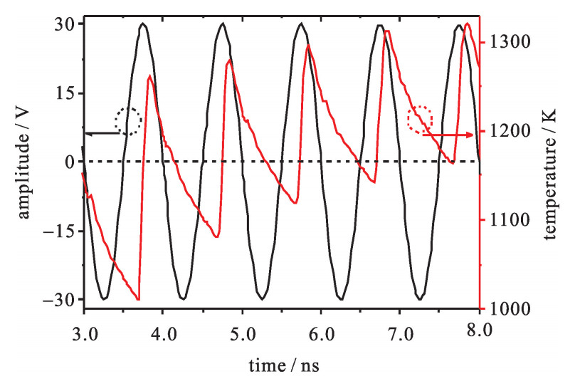
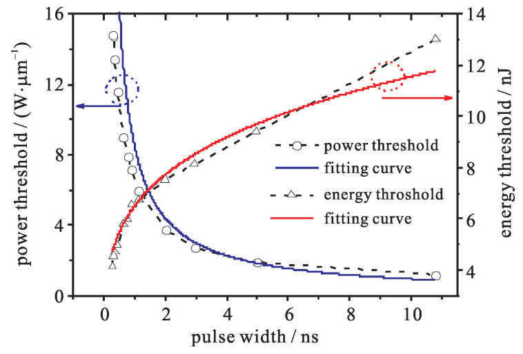
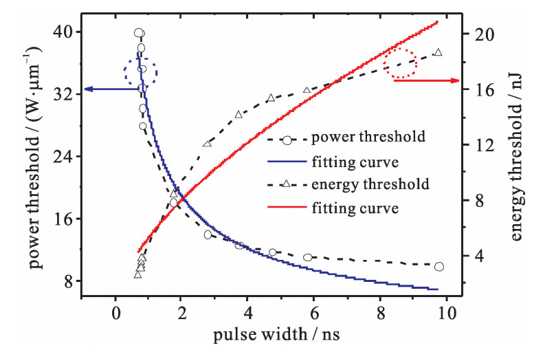
摘要: 建立了PNP型达林顿管的二维电热模型,对处于有源放大区的达林顿管的集电极注入高功率微波(HPM)和强电磁脉冲(EMP)时的瞬态响应进行了仿真。结果表明:HPM注入下,器件内部的峰值温度呈周期性的“下降-上升”,温度升高过程发生在信号的正半周,靠近达林顿管发射极的晶体管发射结边缘是最易毁伤处;EMP注入下,其损伤机理与HPM注入时的正半周时相似,器件内部峰值温度一直上升,易毁伤部位与HPM注入时相同。得到了损伤功率阈值和损伤能量阈值与损伤脉宽的关系,这两种干扰注入下的损伤能量阈值-脉宽关系和损伤功率阈值-脉宽关系公式相似,并且在相同脉宽下,HPM注入下的损伤能量阈值大于EMP注入下的损伤能量阈值。Abstract: A two-dimensional electron-thermal model of the PNP type Darlington tube is established, and the transient behaviors of the Darlington tube in the forward-active region are simulated with the injection of high power microwaves (HPMs) and electromagnetic pulses (EMPs) from the collector. A discussion and a comparison of the damage effects and the mechanism of the device under the injection of HPMs and EMPs are performed. The results show that temperature variation has a periodic rule of "decrease-increase" and temperature elevation occurs in the positive half-period, and the cylindrical region of base-emitter junction of the second transistor (near the emitter of the Darlington tube) is susceptible to damage when HPM signals are injected. While temperature keeps rising and the rate of increase presents a tendency of "rapid-slow" until the device burns out under the injection of EMP signals, and the damage location is the same as the damage area of HPM injection. In addition, the damage mechanism during the positive half-period of HPM injection is similar to that of EPM injection. Finally, the dependence relations of damage energy and damage power of EMPs and HPMs on pulse-width are obtained in a nanosecond range. It is demonstrated that energy threshold increase slowly while power threshold decrease with the increasing of pulse-width.
-
Key words:
- Darlington tube /
- high power microwave /
- electromagnetic pulse /
- pulse width effect
-
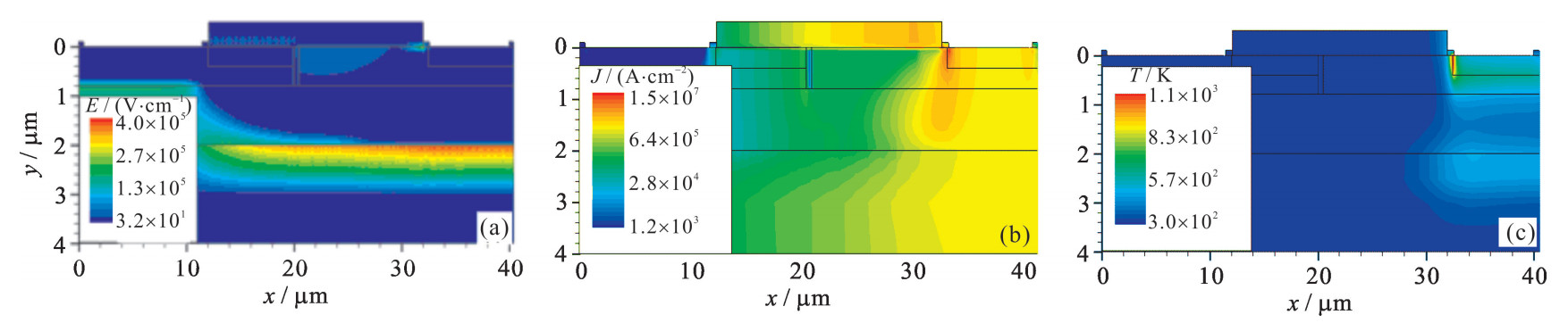
Figure 4. Distribution of (a) electric field, (b) current density and (c) temperature at 3.15 ns
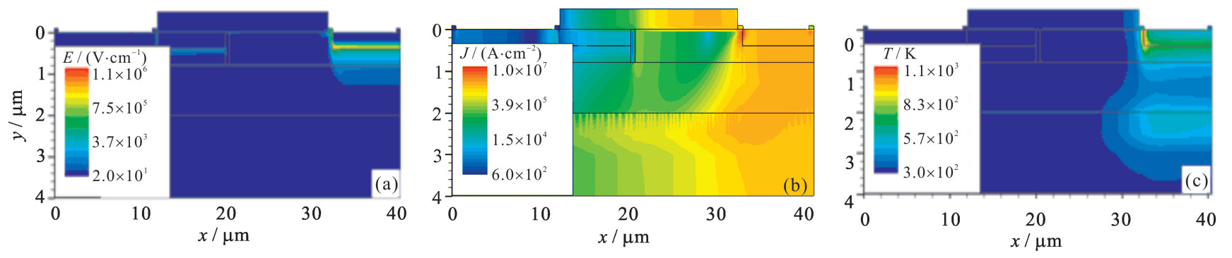
Figure 5. Distribution of (a) electric field, (b) current density and (c) temperature at 3.75 ns
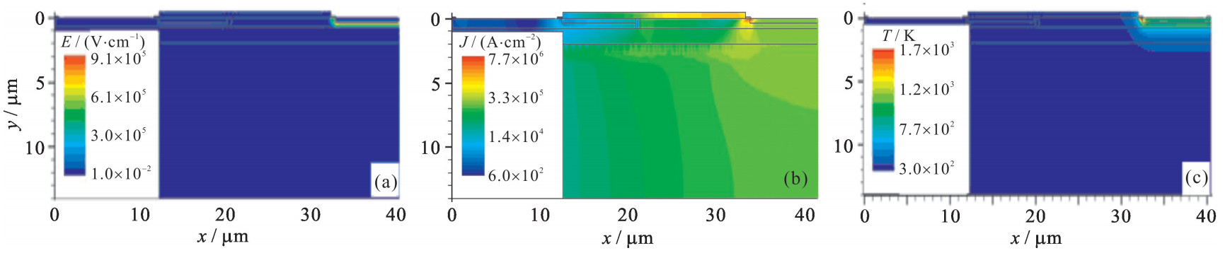
Figure 7. Distribution of (a) electric field, (b) current density and (c) temperature at burn-out time
-
[1] Kim K, Iliadis A A. Operational upsets and critical new bit errors in CMOS digital inverters due to high power pulsed electromagnetic interference[J]. Solid-State Electronics, 2010, 54(1): 18-21. doi: 10.1016/j.sse.2009.09.006 [2] Iliadis A A, Kim K. Theoretical foundation for upsets in CMOS circuit due to high-power electromagnetic interference[J]. IEEE Trans Device Mater Reliab, 2010, 10(3): 347-352. doi: 10.1109/TDMR.2010.2050692 [3] Chai Changchun, Xi Xiaowen, Ren Xingrong, et al. The damage effect and mechanism of the bipolar transistor induced by the intense electromagnetic pulse[J]. Acta Physica Sinica, 2010, 59(11): 8118-8124. doi: 10.7498/aps.59.8118 [4] Wang Haiyang, Li Jiayin, Li Hao, et al. Experimental study and SPICE simulation of CMOS inverters latch-up effects due to high power microwave interference[J]. Prog Electromagn Res, 2008, 87: 313-330. [5] Mansson D, Thottappillil R, Backstrom M, et al. Susceptibility of civilian GPS receivers to electromagnetic radiation[J]. IEEE Trans Electromagn Compat, 2008, 50(1): 434-437. [6] You Hailong, Lan Jianchun, Fan Juping, et al. Research on characteristics degradation of n-metal-oxide-semiconductor field-effect transistor induced by hot carrier effect due to high power microwave[J]. Acta Physica Sinica, 2012, 61: 108501. doi: 10.7498/aps.61.108501 [7] Backstrom M G, Lovstrand K G. Susceptibility of electronic systems to high-power microwave: summary of test experience[J]. IEEE Trans Electromagn Compat, 2004, 46(3): 396-403. doi: 10.1109/TEMC.2004.831814 [8] Nitsch D, Camp M, Sabath F, et al. Susceptibility of some electronic equipment to HPEM threats[J]. IEEE Trans Electromagn Compat, 2004, 46(3): 380-387. doi: 10.1109/TEMC.2004.831842 [9] Li P, Liu Guozhi, Huang Wenhua, et al. The mechanism of HPM pulse-duration damage effect on semiconductor component[J]. High Power Laser and Particle Beams, 2001, 13(3): 353-356. http://www.hplpb.com.cn/article/id/1626 [10] Fan Juping, Zhang Ling, Jia Xinzhang. HPM damage mechanism on bipolar transistors[J]. High Power Laser and Particle Beams, 2010, 22(6): 1319-1322. doi: 10.3788/HPLPB20102206.1319 [11] Ma Zhenyang, Chai Changchun, Ren Xingrong, et al. The damage effect and mechanism of the bipolar transistor caused by microwaves[J]. Acta Physica Sinica, 2012, 61: 078501. doi: 10.7498/aps.61.078501 [12] Ren Xingrong, Chai Changchun, Ma Zhenyang, et al. The damage effect and mechanism of bipolar transistors induced by injection of electromagnetic pulse from the base[J]. Acta Physica Sinica, 2013, 62: 068501. doi: 10.7498/aps.62.068501 [13] Chai Changchun, Zhang Bing, Ren Xingrong, et al. Injection damage of the integrated silicon low-noise amplifier[J]. J Xidian Univ, 2010, 37(5): 898-903. [14] Chai Changchun, Yang Yintang, Zhang Bing, et al. Mechanism of energy-injection damage of silicon bipolar low-noise amplifiers[J]. Semicond Sci Technol, 2008, 29: 035003. [15] 2004 ISE-TCAD Dessis simulation user's manual[M]. Zurich: Integrated Systems Engineering Corp, 2004. [16] Radasky W A. Protection of commercial installations from the high-frequency electromagnetic threats of HEMP and IEMI using IEC standards[C]//Asia-Pacific Symposium on Electromagnetic Compatibility. 2010: 758-761. [17] Jayant B B, Ghandhi S K. Analytical solutions for the breakdown voltage of abrupt cylindrical and spherical junctions[J]. Solid State Electronics, 1976, 19(9): 739-744. doi: 10.1016/0038-1101(76)90152-0 [18] Wunsch D C, Bell R R. Determination of threshold failure levels of semiconductor diodes and transistors due to pulse voltages[J]. IEEE Trans Nucl Sci, 1968, 15(6): 244-259. doi: 10.1109/TNS.1968.4325054 [19] Tasca D M. Pulse power failure modes in semiconductors[J]. IEEE Trans Nucl Sci, 1970, 17(6): 364-372. doi: 10.1109/TNS.1970.4325819 [20] Brown W D. Semiconductors device degradation by high amplitude current pulses[J]. IEEE Trans Nucl Sci, 1972, 19(6): 68-75. doi: 10.1109/TNS.1972.4326810 -

 下载:
下载:


 点击查看大图

图(9)
计量
- 文章访问数: 1106
- HTML全文浏览量: 276
- PDF下载量: 81
- 被引次数: 0
