

Surface analysis after working with rare earth tungsten electrode for high-power pulsed Xenon lamp
-
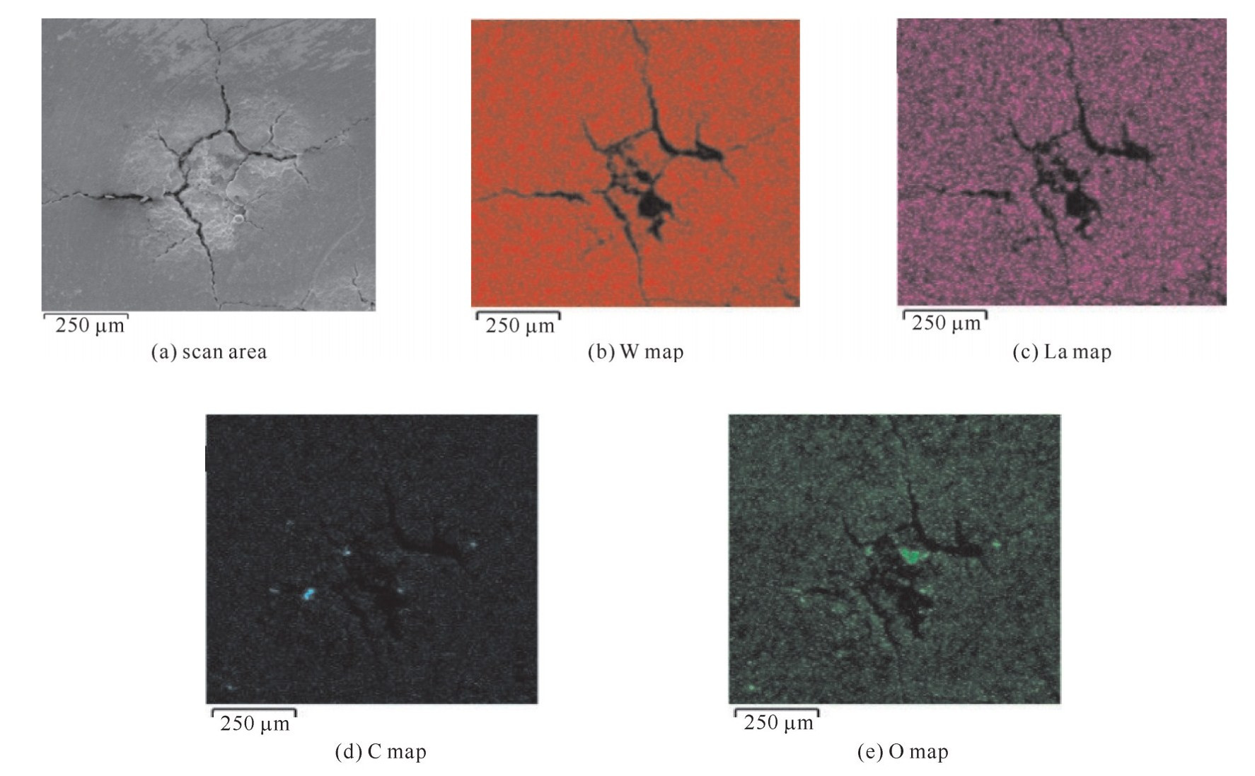
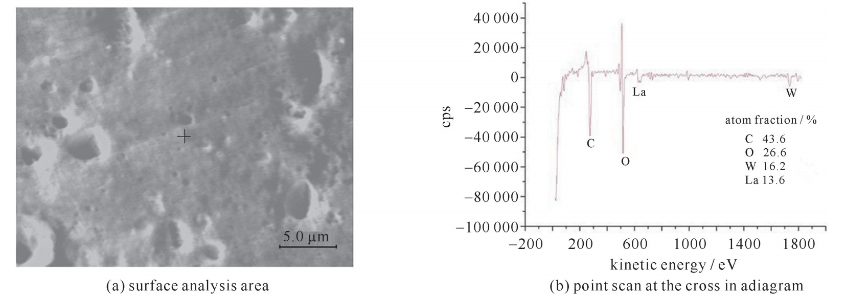
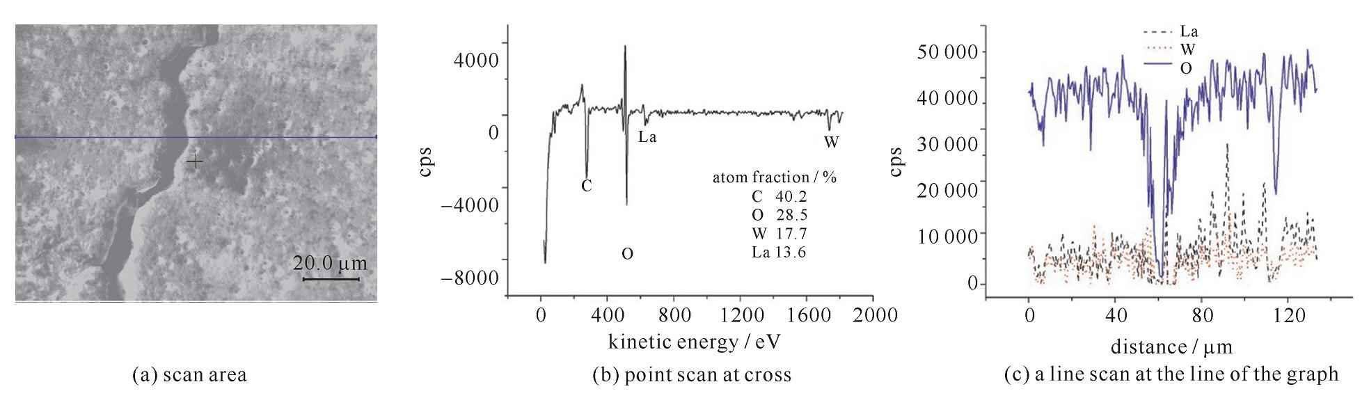
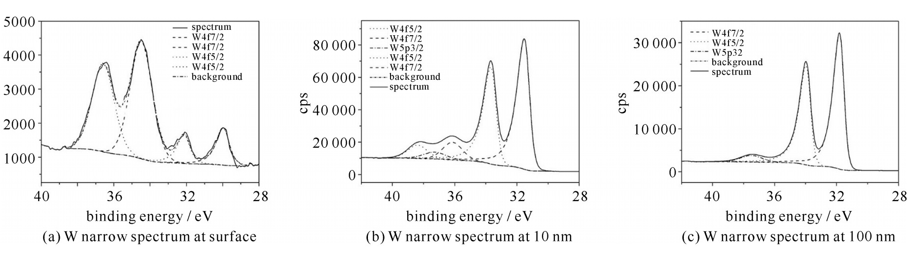
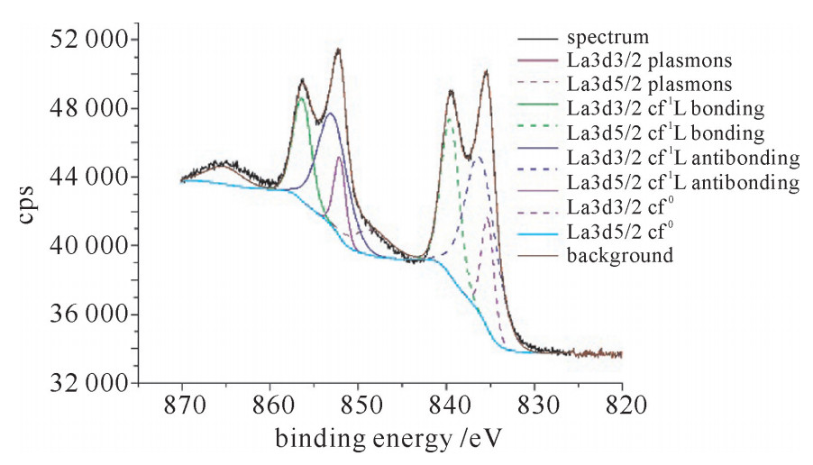
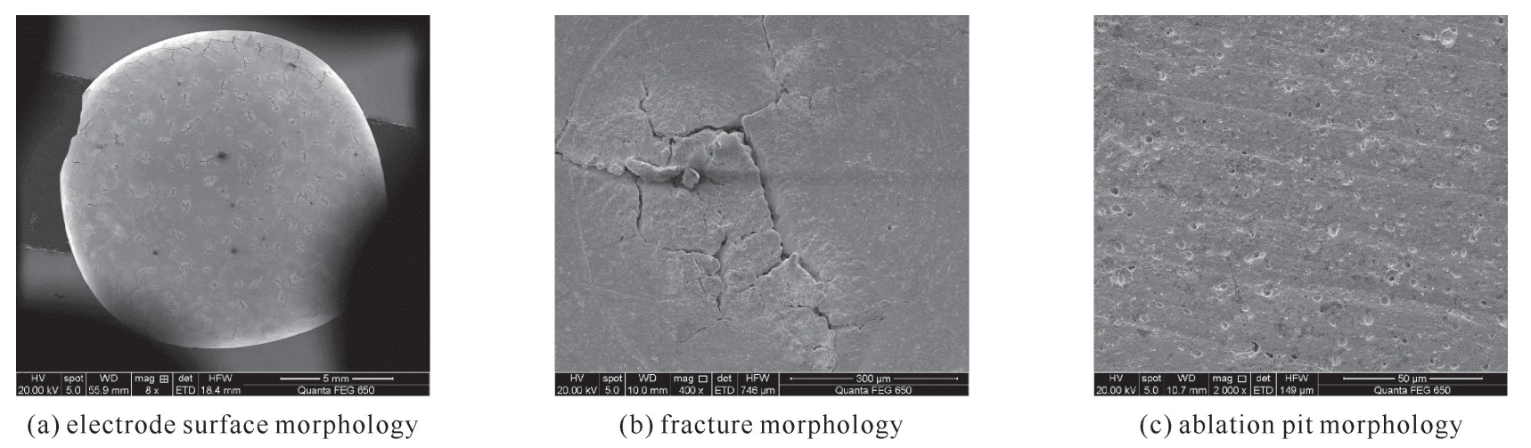
摘要: 为探讨电极表面发生变化的原因和烧蚀机理,为提升电极工作稳定性提供理论依据,分析了经过上万发次点灯测试的大功率脉冲氙灯稀土钨电极的表面形貌、元素深度分布及价态。结果表明:工作后的电极表面出现大量裂纹以及烧蚀坑;表面各元素主要由W, La, O三种元素组成,分布均匀;电极表面La以La3+形式存在,W存在原子态和+6价两种价态,占比分别为18.29%和81.71%;随刻蚀深度增加后,La的价态仍为+3价,W6+迅速减少直至W价态全部变为W0。Abstract: The material selected for the experiment is the high power pulsed Xenon lamp rare earth tungsten electrode after operation. Analysis of appearance, element distribution and elemental valence of rare earth tungsten electrode surface and etched at different depths. Experimental results show that: After the work, there were many cracks on the surface of the electrode and ablation pits. The elements on the surface were evenly distributed and consisted of three elements: W, La, and O.The electrode surface La exists in the form of La3+, W has two valence states W0 and W6+, where W6+ accounts for the majority; After the ion etching, the valencestate of La is still La3+, W still has two types of W0 and W6+, but W0 accounts for the most; After the etching depth increases, the valence state of tungsten becomes W0.
-
Key words:
- rare earth tungsten electrode /
- surface appearance /
- element distribution /
- valence state
-
New parametric current transformers (NPCTs) are widely used to measure beam current in accelerators. Two "In-air-175" NPCTs from Bergoz Instrumentation[1] are selected for BEPCⅡelectron and positron ring. Current sensors are located on a vacuum chamber which has a ceramic break for avoiding the wall current from passing through[2]. The ceramic gap works as a capacity and determines the cutoff frequency. The positron NPCT will heat in the collider mode when the beam current is beyond 500 mA. To solve this problem, a series of studies and researches have been done.
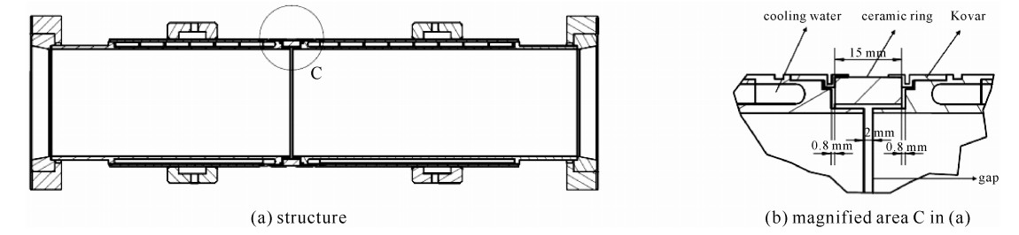
1. Mechanical structure of NPCT vacuum chamber
As the primary study indicates, the heating is quite relevant to the mechanical structure of NPCT. The BEPCⅡ NPCT vacuum chamber profile is shown in Fig. 1. The components of the NPCT vacuum chamber structure are listed in Table 1. An interlayer of water has been designed for cooling, the inlet and outlet of water near the flange side are not shown in Fig. 1. Kovar rings are used to seal the ceramic and the steel chamber. Two extend slices are made to avoid discharge and to protect the ceramic ring and the welding edge.
 Figure 1. NPCT vacuum chamber structureTable 1. Vacuum chamber parameters
component material data pipe steel 316 inner diameter: 96 mm, outer diameter: 111 mm water interlayer water thickness: 2 mm ceramic gap 95%Al2O3 width: 15 mm seal ring Kovar \\ | Show Table DownLoad:
CSV
DownLoad:
CSV
2. Heating problem and solutions
The positron ring NPCT's heating problem arose in 2013 when BEPCⅡ ran at high current collider mode. There were six PT100 temperature sensors: one was on the NPCT sensor, one was on the vacuum chamber, and the other four were on the water cooling pipe, the cooling water was about 16-20 ℃. When the single bunch current reached 10 mA, the temperature of sensor was over 60℃ and the vacuum chamber was near 50 ℃. In the meantime the water outlet temperature showed insufficient cooling. As the current would go up for getting higher luminosity, heating might become serious and destroy the sensor toroid. There are two reasonable explanations of the heating source: one is the power loss caused by wakefield effect of the discontinuous ceramic break[3], the other is the eddy current loss and the hysteresis loss of high frequency signal in the sensor. Methods have been taken to analyse and solve the problem since then.
2.1 Calculation of power loss of the gap structure
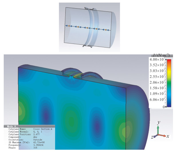
To verify the heating brought by the beam in the gap, a simulation based on CST has been done. As the ceramic gap and the vacuum chamber make a small cavity in a resonator, when charged particles are passing through, they lose energy due to the structure. To calculate the power loss, the loss factor is needed, which can be calculated in CST Particle Studio. A simplified vacuum model inside the chamber is established in CST as shown in Fig. 2. According to BEPCⅡ collider mode, particle sigma is 15 mm, commissioning energy is 1.89 GeV, beta is 0.999 9, and particle path is set in the central of the model. The boundary is set as PEC (perfect electronic conduct). The simulation result shows the loss factor of the structure is 11.2 V/nC.
 Figure 2. CST vacuum model and field distribution of simulation
As the loss factor means voltage loss per charge for a structure, the whole loss power is calculated as[3-4]
Ploss=IQKloss=I2tKlossN (1) where I is mean beam current, N is bunch number, t is revolution time, Kloss is loss factor. For the case I=600 mA, N=72, t=7.9 ns and Kloss=11.2 V/nC, Ploss is about 44 W.
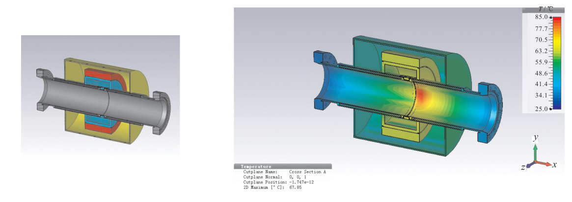
For getting the distribution of the modes, CST Microwave Studio is used to do the TM Eigen mode simulation with frequency up to 15 GHz. The highest field amplitude near the gap is 4×10⁷ V/m at 3.35 GHz as shown in Fig. 2. A complete model includes vacuum chamber, sensor toroid, support and shield is established for post-processing to calculate the temperature. An extreme condition is set that all the power is used for thermal analysis. The material of the shield is copper and the support is Bakelite. In the simulation only natural heat dissipation is included, water cooling is not considered for getting the actual static value, the highest temperature in the chamber is 80 ℃ near the gap. The model and simulation results are shown in Fig. 3.
 Figure 3. NPCT model and static temperature distribution in CST
This simulation only indicates power loss inside the gap, it proves that the structure contributes part of the heating and extra cooling is necessary. The results of the simulation could be a guide for further vacuum chamber design. Making the gap simple and smaller could reduce the loss factor but lead to the reduction of the gap capacity, which will cause the sensor heating problem.
2.2 Sensor heating analysis and solution
Besides the heating on the pipe, the sensor temperature rises, which is a more critical problem to settle. An "S-shaped" copper pipe is designed to wind out of the sensor for cooling water to pass through, but the effect is not obvious, so a fundamental solution is needed.
The NPCT sensor uses finemet cores made of high permeability amorphous alloy thin ribbons [1]. For magnetic materials there is a definition for power loss. Ph is hysteresis loss power, Pe is eddy current loss power, and the loss of the core can be calculated as[5]
W=Wh+We+Wr (2) in which
Wh=f∮HdM (3) We=af2t2Bmax2/ρ (4) and Wr is a loss related to the atomic structure of material, which can be ignored. In equations (3) and (4), f is signal frequency, M is intensity of magnetization, t is core material thickness (which is a constant in our case), Bmax is peak magnetic intensity, a is a constant coefficient, ρ is resistivity of the core. The iron loss of ferromagnetic materials and ferrite is related to frequency (f), f is the key parameter[5].
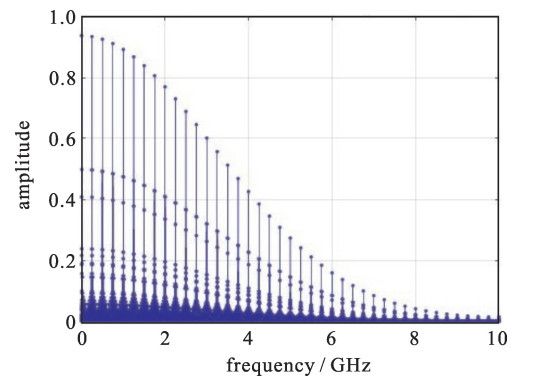
A spectrum of beam for collision mode of BEPCⅡ is simulated in Matlab, with 4 series of 18 bunches in 8 circles. For electron and positron rings with the same bunch mode, they share the same spectrum distribution. As it shows in Fig. 4, the most of the beam power is below 6 GHz. The NPCT bandwidth is DC-10 kHz [1], the higher frequency signal won't be responded and may cause the heating loss.
 Figure 4. Beam spectrum in collision mode
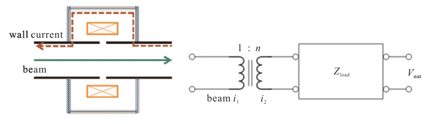
According to the NPCT sensor measurement principle, the mirror current flowing on the vacuum pipe is cut by a ceramic gap. The ceramic gap works like a capacitor, the high frequency of the mirror current passes through the gap, while the low frequency part flows along the outer shielding. The sensor "sees" that Ilow, f=Ibeam-Ihigh, f (I represents beam current, the character "f" in the subscript represents "frequency").
The whole NPCT sensor and front electronics is simplified as an equivalent circuit which is shown in Fig. 5. A transformer theory has been applied in the calculation. The beam current considered is the one turn primary current i1, i2 is the current in the secondary coil (the winding of the output). The electronics and other load are considered as an integrated impedance Zload, so the current reflected impedance Zref can be calculated as in equation (7)[6]
i1=ni2=nVoutZload (5) Zload=nVouti1=nSsensitivity (6) Zref=(1n)2Zload=nSsensitivityn2=Ssensitivityn=0.025Ω (7)  Figure 5. NPCT measurement principle and equivalent circuit
The sensitivity Ssensitivity of NPCT is 5 V/A in BEPCⅡ. The turns ratio n is 200 in 5 V/A range.
The -3 dB point of cutoff frequency is obtained when the impedance of the cavity Zcavity is equal to the impedance of the gap Zgap, the impedance of the wall conduct can be neglected when compare to the transformer reflected impedance Zref, so Zcavity≈Zref[1]. As Z=1/(2π fcuttoffC), the value C of the gap capacitance determines the higher cutoff frequency fcuttoff of the wall current entering into the cavity. Increase C will reduce fcuttoff at certain impedance, which also means reducing the high frequency signal flow through the sensor.
C of the ceramic gap can be approximately calculated as[7]
C=Sε0εcLc=π(r2out−r2in)ε0εcLc≈19pF (8) where the dielectric constant ε0=8.854×10⁻¹², the relative dielectric constant of ceramic εc=9[8], the ceramic ring effective insulation length Lc=10 mm, the outer radius of the ceramic rout=55.5 mm, the inner radius of the ceramic rin=48 mm.
When C is 19 pF, the fcuttoff is over 10 GHz which equals that Ihighf is all over 10 GHz, so Ilowf covers the whole bandwidth of the beam current. Most of the unwanted high frequency signal is "seen" by the sensor and causes the heating.
There are many methods to increase the capacitor, a simple way which does not need to break the vacuum chamber is: put a big parallel capacitor across the ceramic gap, they form a bigger capacitor Cadd. Cadd can be calculated as
Cadd=Sε0εkh=πdLkε0εkh≈8nF (9) where the area of the kapton foil S=27 883.2 mm2, the outer diameter of the vacuum d=111 mm, the length of the kapton foil Lk=80 mm, the thickness of the kapton foil h=110 μm, the relative dielectric constant of kapton foil εk=3.4[9].
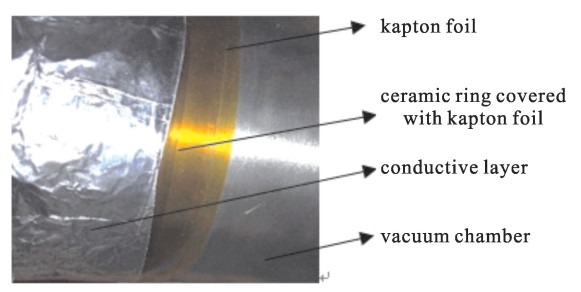
Cadd is parallelly connected with Cceramic, which is small enough to be ignored, fcutoff=1/(2πCZref) deceases to 800 MHz. The high frequency signal which can be seen by the sensor is reduced. In our case, a conductive layer with 110 μm-thick kapton foil is used to wind on the pipe, as shown in Fig. 6. The kapton foil wraps the ceramic, while the conductive layer is partly covered by the kapton foil with only one side stick to the vacuum chamber.
 Figure 6. Kapton foil and conductive layer
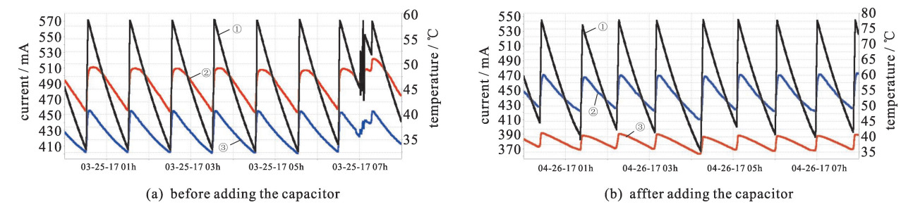
The temperature of the sensor indicates that the method is effective. Before adding capacitor to the gap, temperature of the sensor is much higher than the vacuum chamber. As the history data shown in Fig. 7, sensor temperature is about 50 ℃ (Fig. 7(a)), vacuum chamber temperature is about 40 ℃ (Fig. 7(a)) at 550 mA (peak current in Fig. 7(a)). After adding the capacitor to the gap, temperature of the sensor drops to 40 ℃ (Fig. 7(b)) at 550 mA (peak current in Fig. 7(b)), and the vacuum chamber temperature is 60 ℃ (Fig. 7(b)). Most power has been hold in the chamber for energy conservation. Note that the beam has the same pattern in this operation cycle.
 Figure 7. Beam current(①), sensor temperature(②), chamber temperature(③) before and after adding the capacitor
Definitely, the temperature change contains the above two contributions. Accurate calculation of power transfer needs more considerations.
3. Conclusion and discussion
The heating problem of current transformer (CT) is common in the accelerators, especially in those with high current or complex beam spectrum machines. For overall consideration, the capacitor of the gap should be in nF magnitude or higher for NPCT, and wakefield simulation should be done while designing the gap structure. An experience is that unnecessary slight space should be avoided, but expansion space of ceramic needs to be reserved, because of the thermal effect. A curious situation in BEPCⅡ is that the electron NPCT which has the same condition with the positron one does not meet such serious heating problem for both the gap and the sensors, further study should be carried out.
Acknowledgments: We thank Julien Bergoz from Bergoz Instrumentation for great assistance in this reaserch. We also thank our colleagues in Beam Instrumentation (BI) group who provide expertise that helped the expriment. -
表 1 各种元素在标准状态下的刻蚀速率
Table 1. Etching rates of various elements in the standard state
element sputter rate /(nm/s) W 0.11 Si 0.22 Fe 0.28 Cu 0.18 Mg 0.7 Mo 0.15 Ta 0.127  下载: 导出CSV
-
[1] 向世清. 激光驱动核聚变研究进展[J]. 科学, 2014, 66(5): 22-25. https://www.cnki.com.cn/Article/CJFDTOTAL-KXZZ201405007.htmXiang Shiqing. Progress in laser driven nuclear fusion research. Science, 2014, 66(5): 22-25 https://www.cnki.com.cn/Article/CJFDTOTAL-KXZZ201405007.htm [2] 林尊琪. 激光核聚变的发展[J]. 中国激光, 2010, 37(9): 2202-2207. https://www.cnki.com.cn/Article/CJFDTOTAL-JJZZ201009008.htmLin Zunqi. Development of laser nuclear fusion. Chinese Journal of Lasers 2010, 37(9): 2202-2207 https://www.cnki.com.cn/Article/CJFDTOTAL-JJZZ201009008.htm [3] 张林, 杜凯. 激光惯性约束聚变靶技术现状及其发展趋势[J]. 强激光与粒子束, 2013, 25(12): 3091-3097. http://www.hplpb.com.cn/cn/article/doi/3091Zhang Lin, Du Kai. Current situation and development trend of laser inertial restricted fusion target technology. High Power Laser and Particle Beams, 2013, 25(12): 3091-3097 http://www.hplpb.com.cn/cn/article/doi/3091 [4] 郑万国, 邓颖, 周维, 等. 激光聚变研究中心激光技术研究进展[J]. 强激光与粒子束, 2013, 25(12): 3082-3090. http://www.hplpb.com.cn/cn/article/doi/3082Zheng Wanguo, Deng Ying, Zhou Wei, et al. Progress in laser technology research center. High Power Laser and Particle Beams, 2013, 25(12): 3082-3090 http://www.hplpb.com.cn/cn/article/doi/3082 [5] 刘建军, 李海兵, 郭向朝, 等. 高功率氙灯脉冲放电过程中石英管壁热损伤机理[J]. 强激光与粒子束, 2014, 26: 082004. doi: 10.11884/HPLPB201426.082004LiuJianjun, Li Haibing, GuoXiangchao, et al. Thermal damage mechanism of quartz tube wall during pulse discharge of high power Xenon lamp. High Power Laser and Particle Beams, 2014, 26: 082004 doi: 10.11884/HPLPB201426.082004 [6] 马永波, 彭述明, 龙兴贵, 等. 影响高功率脉冲氙灯寿命的因素[J]. 强激光与粒子束, 2010, 22(10): 2483-2486. http://www.hplpb.com.cn/article/id/4529Ma Yongbo, Peng Shuming, Long Xinggui, et al. Factors affecting the life of high power pulse xenon lamp. High Power Laser and Particle Beams, 2010, 22(10): 2483-2486 http://www.hplpb.com.cn/article/id/4529 [7] 李鹏, 杨建参, 李岩. 几种氙灯用钨阴极抗烧蚀性能的研究[J]. 中国钨业, 2017, 32(3): 59-64. https://www.cnki.com.cn/Article/CJFDTOTAL-ZGWU201703045.htmLi Peng, Yang Jiancan, Li Yan. Study on the corrosion resistance of tungsten cathode for several Xenon lamps. Chinese Tungsten Industry, 2017, 32(3): 59-64 https://www.cnki.com.cn/Article/CJFDTOTAL-ZGWU201703045.htm [8] 吴佳玮, 韩若愚, 丁卫东, 等. 长寿命铜钨合金气体开关电极的烧蚀形貌[J]. 中国电机工程学报, 2017, 37(8): 2465-2478. https://www.cnki.com.cn/Article/CJFDTOTAL-ZGDC201708032.htmWu Jiawei, Han Ruoyu, Ding Weidong, et al. The ablation morphology of long-lived copper tungsten alloy gas switch electrode. Proceedings of the CSEE, 2017, 37(8): 2465-2478 https://www.cnki.com.cn/Article/CJFDTOTAL-ZGDC201708032.htm [9] 姚学玲, 曾正中, 陈景亮. 脉冲电弧对钨铜电极表面侵蚀形态的研究[J]. 高电压技术, 2006, 32(7): 21-24. https://www.cnki.com.cn/Article/CJFDTOTAL-GDYJ200607008.htmYao Xueling, Zeng Zhengzhong, Chen Jingliang, et al. Study on the surface erosion pattern of tungsten copper electrode by pulse arc. High Voltage Engineering, 2006, 32(7): 21-24 https://www.cnki.com.cn/Article/CJFDTOTAL-GDYJ200607008.htm [10] 聂祚仁, 陈颖, 周美玲, 等. 复合稀土氧化物在钨电极中的分布规律和作用机理[J]. 金属学报, 1999(9): 981-984. https://www.cnki.com.cn/Article/CJFDTOTAL-JSXB199909017.htmNie Zuoren, Chen Ying, Zhou Meiling, et al. Distribution law and mechanism of composite rare earth oxide in tungsten electrodes. Acta Metallurgica Sinica, 1999(9): 981-984 https://www.cnki.com.cn/Article/CJFDTOTAL-JSXB199909017.htm [11] 聂祚仁, 周美玲, 张久兴, 等. 稀土钨电极材料研究进展[J]. 材料导报, 1997(5): 19-22. https://www.cnki.com.cn/Article/CJFDTOTAL-CLDB199705005.htmNie Zuoren, Zhou Meiling, Zhang Jiuxing, et al. Research progress on rare earth tungsten electrode materials. Materials Review, 1997(5): 19-22 https://www.cnki.com.cn/Article/CJFDTOTAL-CLDB199705005.htm [12] 周美玲, 聂祚仁, 陈颖, 等. 稀土钨电极研究与应用[J]. 中国钨业, 2000, 15(1): 30-34. https://www.cnki.com.cn/Article/CJFDTOTAL-ZGWU200001009.htmZhou Meiling, Nie Zuoren, Chen Ying, et al. Research and application of rare earth tungsten electrode. Chinese Tungsten Industry, 2000, 15(1): 30-34 https://www.cnki.com.cn/Article/CJFDTOTAL-ZGWU200001009.htm [13] 杨建参, 聂祚仁, 周美玲, 等. 稀土钨电极材料的研究[J]. 中国钨业, 2007, 22(1): 39-41. https://www.cnki.com.cn/Article/CJFDTOTAL-ZGWU200701010.htmYang Jiancan, Nie Zuoren, Zhou Meiling, et al. Study on rare earth tungsten electrode materials. Chinese Tungsten Industry, 2007, 22(1): 39-41 https://www.cnki.com.cn/Article/CJFDTOTAL-ZGWU200701010.htm [14] Krasovskii P V, Malinovskaya O S, Samokhin A V, et al. XPS study of surface chemistry of tungsten carbides nanopowders produced through DC thermal plasma/hydrogen annealing process[J]. Applied Surface Science, 2015, 339(1): 46-54. [15] Polášek J, Mašek K, Marek A, et al. Effects of oxygen addition in reactive cluster beam deposition of tungsten by magnetron sputtering with gas aggregation[J]. Thin Solid Films, 2015, 591(s2): 194-199. [16] Xie F Y, Gong L, Liu X, et al. XPS studies on surface reduction of tungsten oxide nanowire film by Ar+, bombardment[J]. Journal of Electron Spectroscopy & Related Phenomena, 2012, 185(3/4): 112-118. [17] Sunding M F, Hadidi K, Diplas S, et al. XPS characterisation of in situ, treated lanthanum oxide and hydroxide using tailored charge referencing and peak fitting procedures[J]. Journal of Electron Spectroscopy & Related Phenomena, 2011, 184(7): 399-409. [18] Zhao M, Lian J, Yu H, et al. Dielectric functions of La-based cuprate superconductors for visible and near-infrared wavelengths[J]. Applied Surface Science, 2017, 421. [19] Oliveira R C, Hammer P, Guibal E, et al. Characterization of metal-biomass interactions in the lanthanum(Ⅲ) biosorption on Sargassum sp. using SEM/EDX, FTIR, and XPS: Preliminary studies[J]. Chemical Engineering Journal, 2014, 239(3): 381-391. [20] Krishnan R V, Mittal V K, Babu R, et al. Heat capacity measurements and XPS studies on uranium-lanthanum mixed oxides[J]. Journal of Alloys & Compounds, 2011, 509(7): 3229-3237. 期刊类型引用(1)
1. 范庆梅,刘佰奇,李琦,黄金印,何平,张红星,周宇鹏,魏然,李国广. 环路热管式光子吸收器的换热可行性. 强激光与粒子束. 2022(04): 110-114 .  本站查看
本站查看其他类型引用(0)
-

 DownLoad:


 点击查看大图
计量
- 文章访问数: 1299
- HTML全文浏览量: 311
- PDF下载量: 123
- 被引次数: 1
