

Parameter extraction technique of millimeter wave small-signal equivalent circuit model of 45 nm MOSFET
-
摘要: 为了有效地表征45 nm MOSFET毫米波频段下的电学特性,研究了其高频等效电路的建模方法。基于45 nm MOSFET的器件物理结构及其导纳参数分析,通过综合考虑器件的本征物理特性、管脚及测试寄生特性,提出了一种准静态近似的高频等效电路模型及其参数直接提取的高精度简化算法,以此来统一表征模型参数从强反型区到弱反型区的偏置依赖性,并使之在不同偏置条件下的特性表征具有良好的连续性,以便于移植到商业仿真设计自动化工具中。通过ADS2013仿真工具的散射参数模拟结果与测量数据的一致性比较,验证了所建模型的实用性及其参数提取算法的准确性, 并表征了45 nm器件的偏置依赖性。Abstract: With the development of channel down-scaling of low-voltage low-power CMOS technology, the optimal operation points are shown to shift from the strong inversion toward lower moderated inversion and weak inversion regimes. High-frequency equivalent circuit modeling is a prerequisite for finding the physical mechanism of MOSFET device, and is essential for the HF integrated circuits. Based on the physical structure of 45 nm MOSFET device and its Y parameters analysis, a quasi-static approximate RF equivalent circuit model and its high-precision simplified parameter extraction algorithm is proposed by taking into account the intrinsic physical characteristics of the device, the electromagnetic characteristics of the pin and the parasitic characteristics of the test pad and test interconnects, which are used to describe the bias dependence from the strong inversion and weak inversion regimes. Therefore, the device characterizations offer excellent accuracy, continuity and smoothness under different bias condition, and can be easily implanted into commercial EDA tools. Direct extraction method is performed by S-parameter analysis including the intrinsic and the extrinsic components and the substrate-related effect. Finally, the practicability and the accuracy of the proposed model and its parameters extract algorithm are verified by the consistency comparison of the simulated results by using ADS2013 tool and the measured S parameters. The experimental results show the bias dependence of 45nm MOSFET.
-
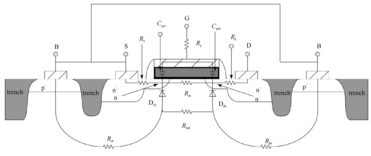
图 1 NMOSFET等效电路参数的物理结构表征
Figure 1. Physical structure characterization of NMOSFET equivalent electrical parameters
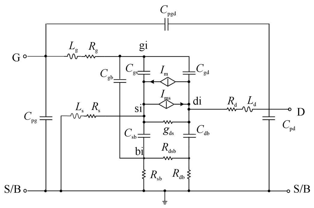
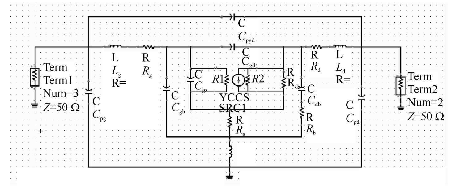
图 2 MOSFET的毫米波小信号等效电路
Figure 2. Millimeter wave small signal equivalent circuit of MOSFET
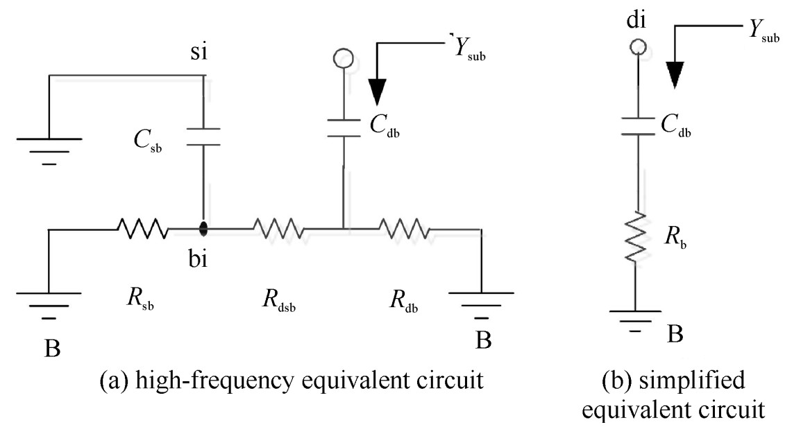
图 3 衬底网络的高频等效电路和简化等效电路
Figure 3. High-frequency equivalent circuit and simplified equivalent circuit of substrate network
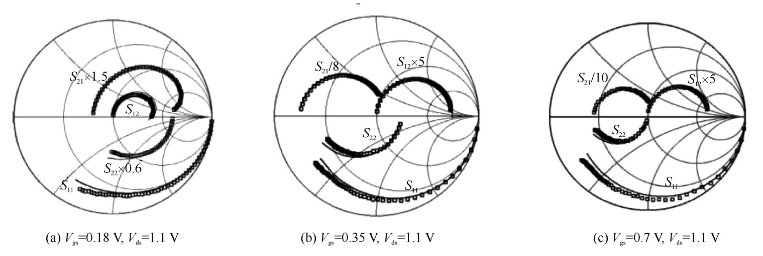
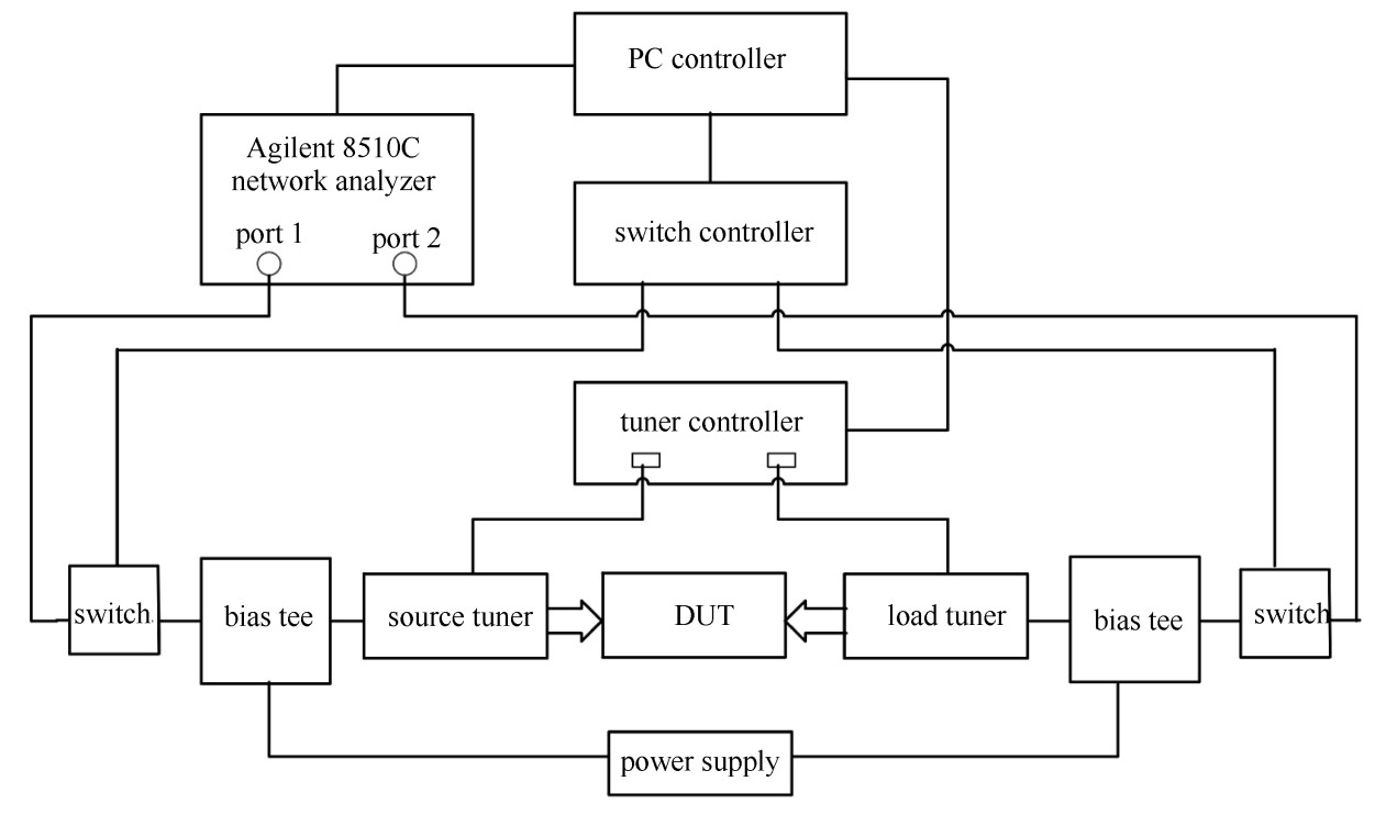
图 15 1~50 GHz测量与模拟的S参数比较
Figure 15. Comparison of measurement and simulation of S parameters from 1 to 50 GHz
(the symbol shows measurement results, the curve shows simulation results)
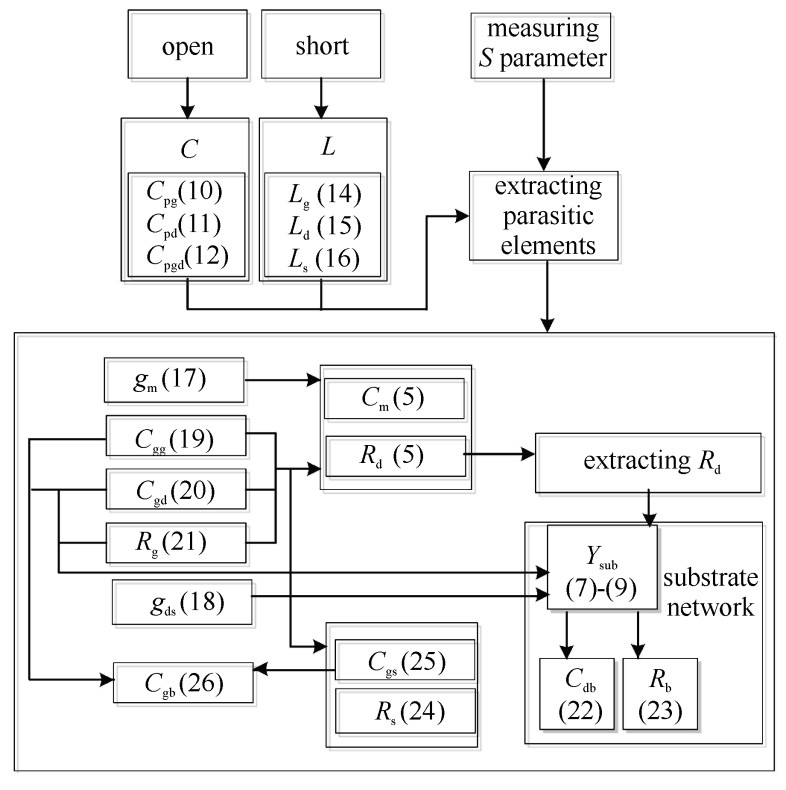
表 1 不同偏置下器件小信号等效电路参数的提取结果
Table 1. Extracted results of device small signal equivalent circuit parameters for different bias
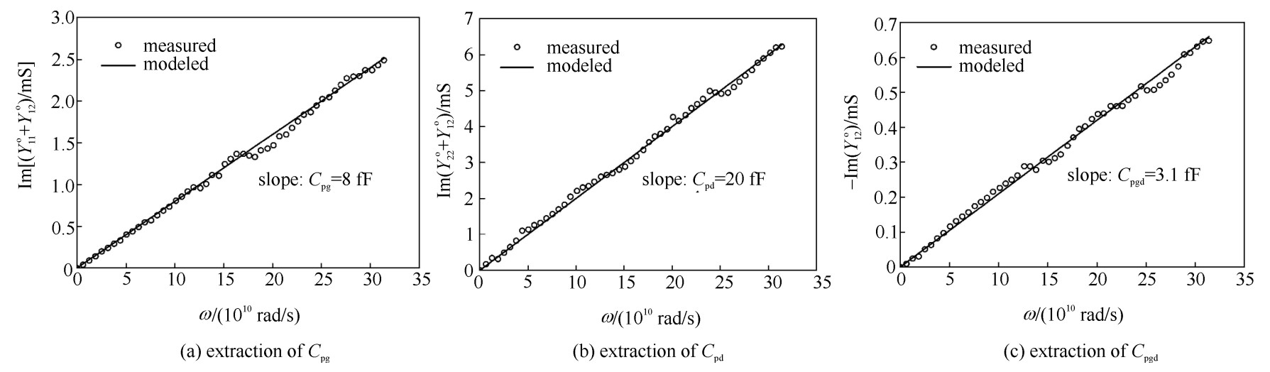
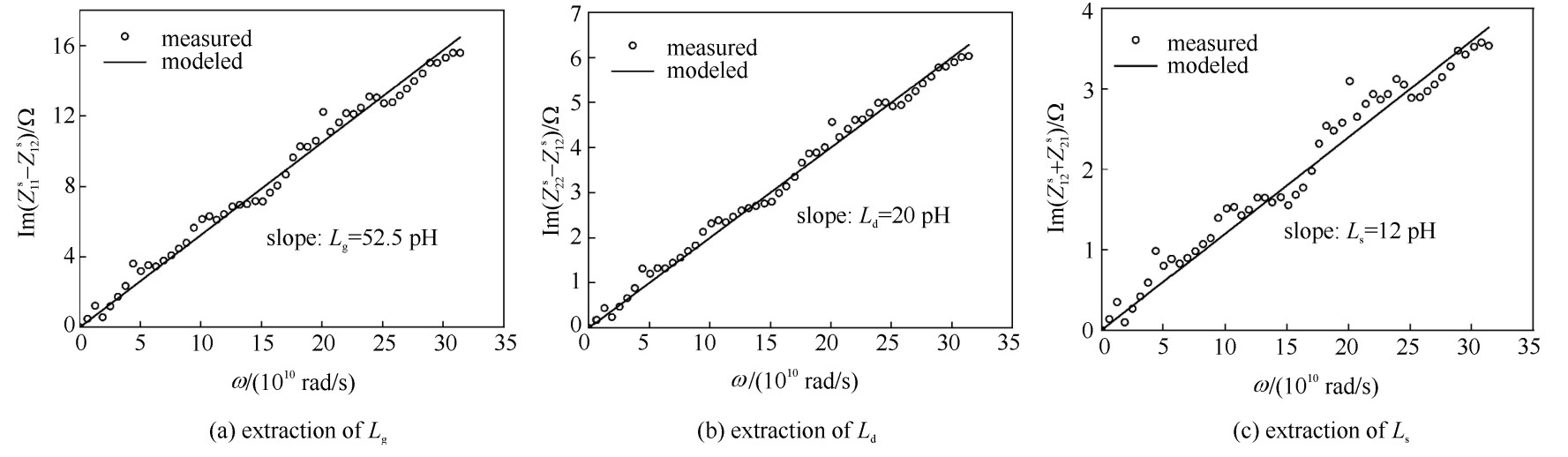
region Vgs /V Vds /V Cpg/fF Cpd/fF Cpgd/fF Lg/pH Ld/pH Ls/pH Rg/Ω Rs/Ω Rd/Ω weak inversion
(0~0.22)V0.1 1.1 8 20 2.1 52.5 20 12 3.98 0.378 0.306 0.2 1.1 8 20 2.1 52.5 20 12 3.98 0.378 0.306 middle inversion
(0.22~0.53)V0.3 1.1 8 20 2.1 52.5 20 12 3.98 0.378 0.306 0.5 1.1 8 20 2.1 52.5 20 12 3.98 0.378 0.306 strong inversion
(0.53~1.2)V1.1 1.1 8 20 2.1 52.5 20 12 3.98 0.378 0.306 region Vgs /V Vds /V Cdb/fF Rb/Ω Cgg/fF Cgs/fF gds/ms gm/ms Cm/fF Cgd/fF Cgb/fF weak inversion
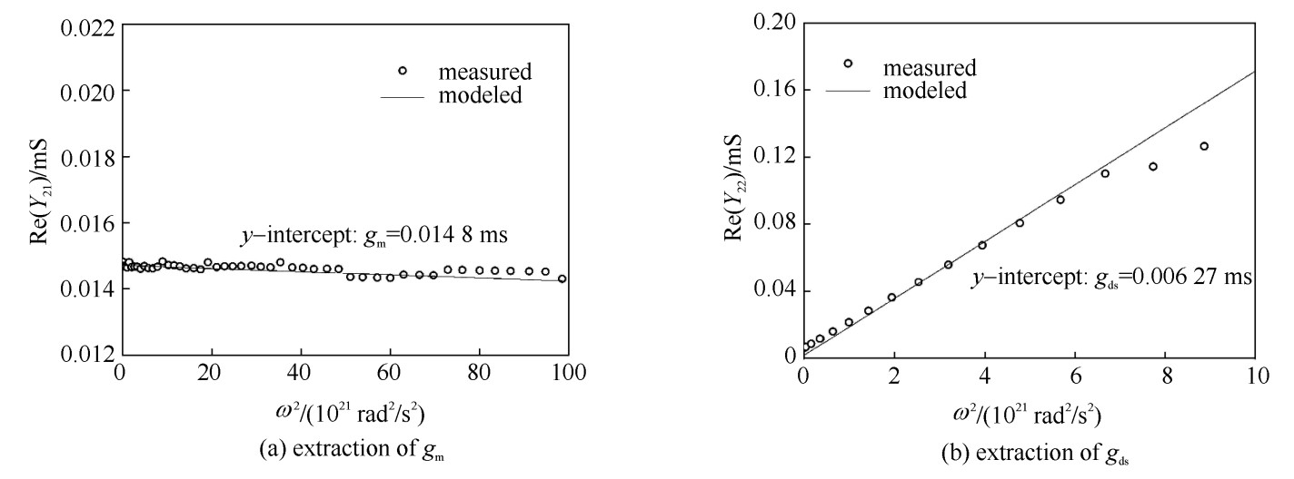
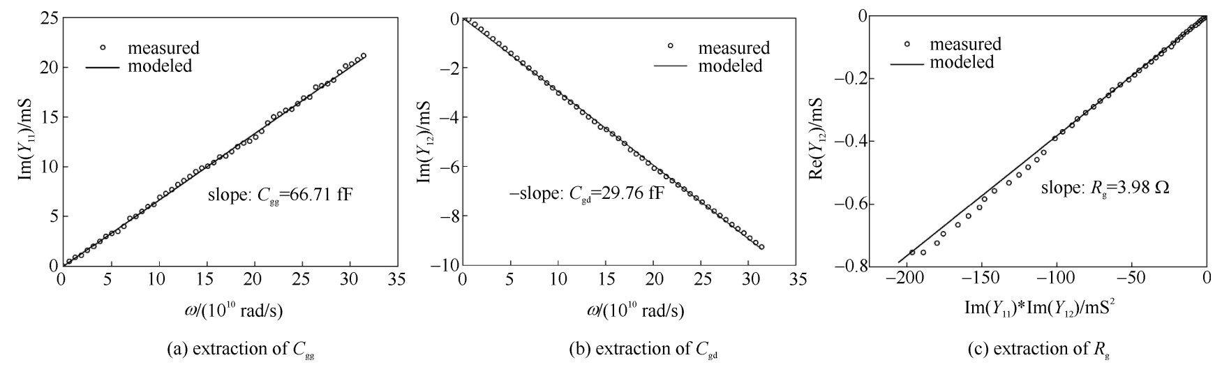
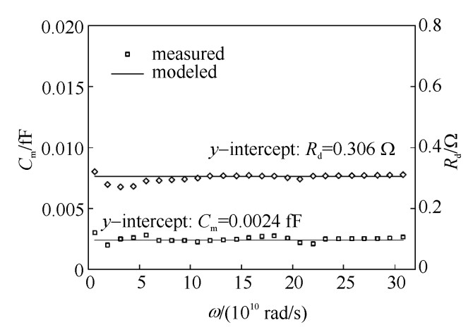
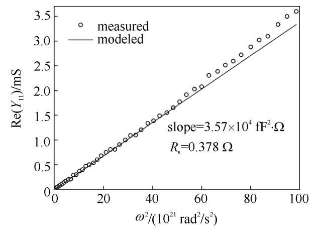
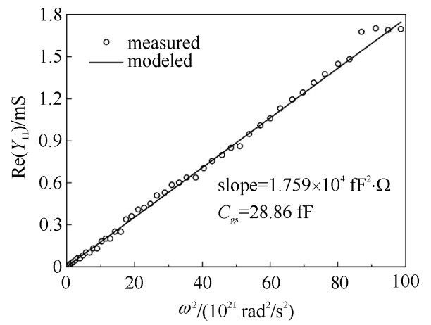
(0~0.22)V0.1 1.1 18.10 40.56 66.71 28.86 0.006 27 0.014 8 0.002 4 29.76 0.31 0.2 1.1 18.86 31.29 69.19 37.31 1.628 0.580 95 2.01 29.76 0.56 middle inversion
(0.22~0.53)V0.3 1.1 20.83 18.11 79.36 47.70 5.86 5.0873 14.50 29.70 2.10 0.5 1.1 21.33 6.30 83.33 56.50 12.30 38.685 7 25.00 29.64 2.89 strong inversion
(0.53~1.2)V1.1 1.1 21.33 1.06 94.24 62.68 19.90 110.648 32.30 31.00 4.11  下载: 导出CSV
-
[1] Parvizi M, Allidina K, El-Gamal M N. A sub-mW, ultra-low-voltage, wideband low-noise amplifier design technique[J]. IEEE Trans Very Large Scale Integration Systems, 2015, 23(6): 1111-1122. doi: 10.1109/TVLSI.2014.2334642 [2] Do A V, Boon C C, Do M A, et al. A subthreshold low-noise amplifier optimized for ultra-low-power applications in the ISM band[J]. IEEE Trans Microwave Theory & Techniques, 2008, 56(2): 286-292. https://dr.ntu.edu.sg/handle/10220/4678 [3] 王军, 戴逸松. 低噪声前放中集成运放电路的En-In噪声性能分析[J]. 仪器仪表学报, 1998, 19(4): 352-357. doi: 10.3321/j.issn:0254-3087.1998.04.004Wang Jun, Dai Yisong. En-In noise performance analysis of integrated operational circuit in low-noise preamplifier. Chinese Journal of Scientific Instrument, 1998, 19(4): 352-357 doi: 10.3321/j.issn:0254-3087.1998.04.004 [4] Lee C I. An improved cascade-based noise deembedding method for on-wafer noise parameters measurements[J]. IEEE Trans Electron Devices Letters, 2015, 36(4): 291-293. doi: 10.1109/LED.2015.2405915 [5] Yeh K L. Narrow-width effect on high-frequency performance and RF noise of sub-40-nm multifinger nMOSFETs and pMOSFETs[J]. IEEE Transactions on Electron Devices, 2013, 60(1): 109-116. doi: 10.1109/TED.2012.2228196 [6] 王军, 王林, 王丹丹. 40 nm金属氧化物半导体场效应晶体管感应栅极噪声及互相关噪声频率与偏置依赖性建模[J]. 物理学报, 2016, 65: 237102. doi: 10.7498/aps.65.237102Wang Jun, Wang Lin, Wang Dandan. Frequency and bias dependent modeling of induced gate noise and cross-correlation noise in 40 nm metal-oxide-semiconductor field-effect transistors. Acta Physica Sinica, 2016, 65: 237102 doi: 10.7498/aps.65.237102 [7] Enz C C, Cheng Y. MOS transistor modeling for RF IC design[J]. IEEE Journal of Solid-State Circuits, 2000, 35(2): 186-201. doi: 10.1109/4.823444 [8] Cheng Yuhua. MOSFET modeling for RF IC design[J]. IEEE Trans Electron Devices, 2005, 52(7): 1286-1303. doi: 10.1109/TED.2005.850656 [9] Poulain L, Waldhoff N, Gloria D, et al. Small signal and HF noise performance of 45 nm CMOS technology in mmW range[C]//IEEE Radio Frequency Integrated Circuits Symposium. 2011: 1-4. [10] Enz C. An MOS transistor model for RF IC design valid in all regions of operation[J]. IEEE Trans Microwave Theory & Techniques, 2002, 50(1): 342-359. https://ieeexplore.ieee.org/document/981286 [11] Chan L H K, Yeo K S, Chew K W J, et al. High-frequency noise modeling of MOSFETs for ultra low-voltage RF applications[J]. IEEE Trans Microwave Theory & Techniques, 2015, 63(1): 141-154. https://www.sciencedirect.com/science/article/pii/S0038110198001920 [12] Chalkiadaki M A, Enz C C. RF small-signal and noise modeling including parameter extraction of nanoscale MOSFET from weak to strong inversion[J]. IEEE Trans Microwave Theory & Techniques, 2015, 63(7): 1-12. https://ieeexplore.ieee.org/document/7109953/ [13] Enz C C, Vittoz E A. Charge-based MOS transistor modeling: The EKV model for low-power and RF IC design[M]. New York: John Wiley, 2006. [14] Issaoun A, Xiong Y Z, Shi J, et al. On the deembedding issue of CMOS multigigahertz measurements[J]. IEEE Trans Microwave Theory & Techniques, 2007, 55(9): 1813-1823. [15] Frickey D A. Conversions between S, Z, Y, H, ABCD, and T parameters which are valid for complex source and load impedances[J]. IEEE Trans Microwave Theory & Techniques, 1994, 42(2): 205-211. https://ieeexplore.ieee.org/document/275248/ -


 点击查看大图
计量
- 文章访问数: 1243
- HTML全文浏览量: 292
- PDF下载量: 130
- 被引次数: 0
