System-level electrostatic discharge simulation based on transmission line pulse modeling
-
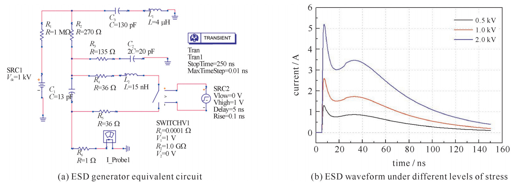
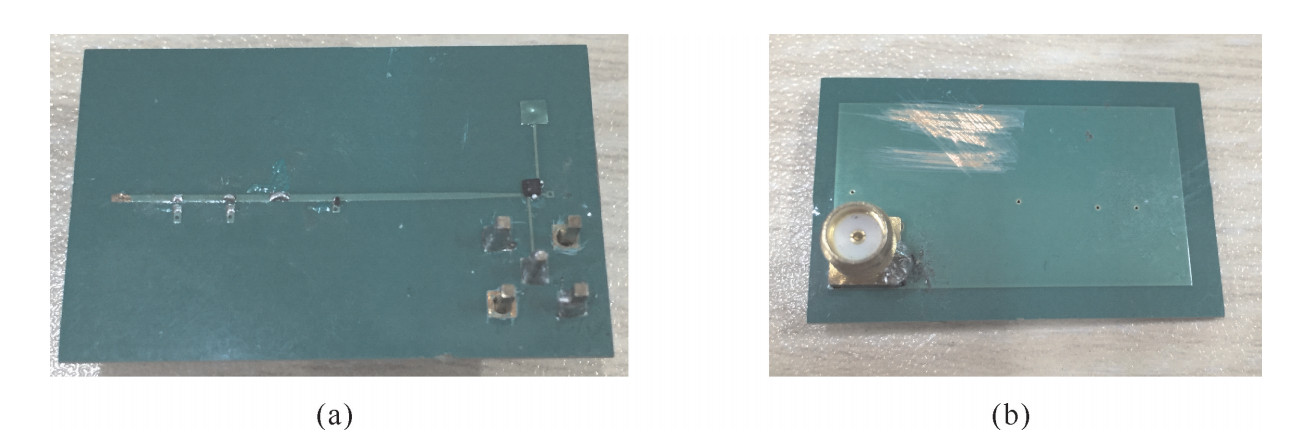
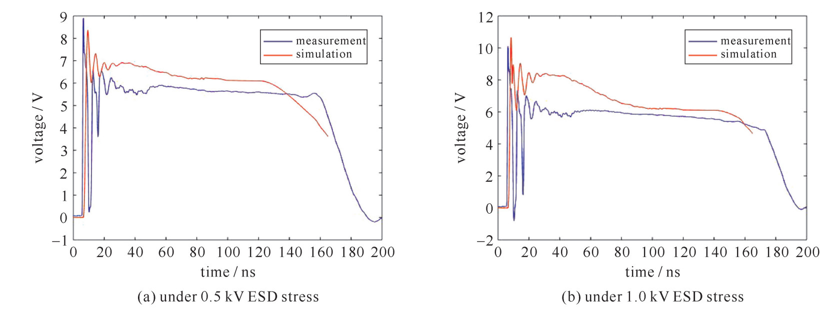
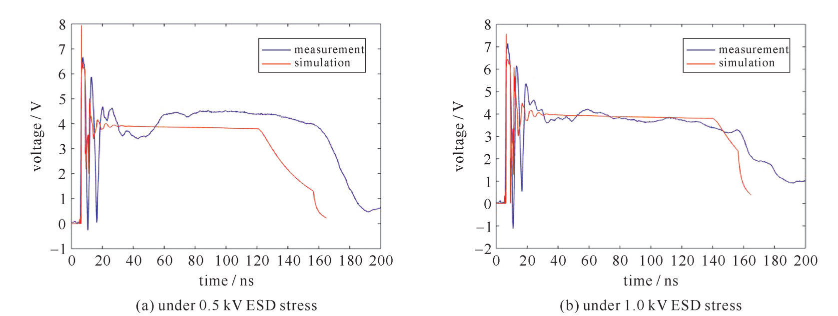
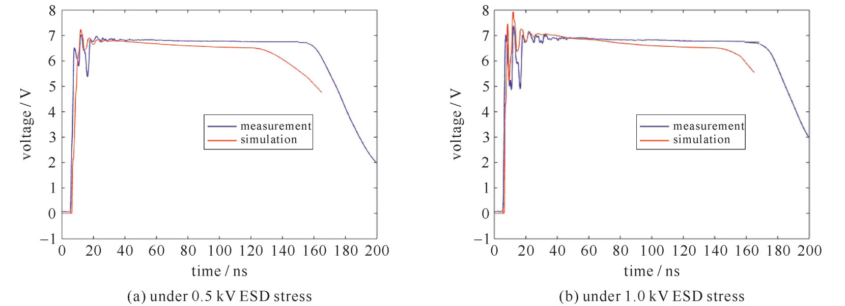
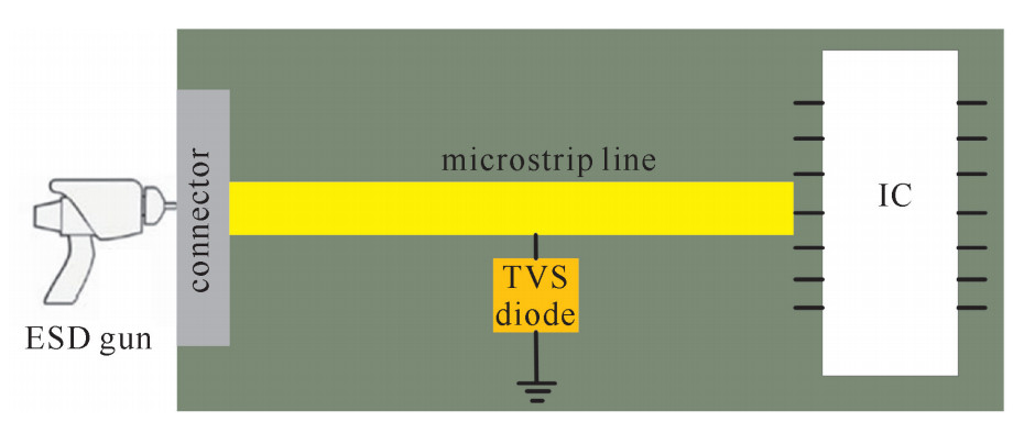
摘要: 系统级静电放电(ESD)效应仿真可以在电子系统进行测试之前进行有效的静电放电效应防护,缩短研发周期。根据传输线脉冲测试(TLP)结果,对瞬态电压抑制(TVS)二极管和芯片引脚进行spice行为建模,结合ESD脉冲源的等效电路模型,PCB板的S参数模型,采用场路协同技术完成了系统级静电放电效应的仿真。针对一个典型的电子系统,在IEC 61000-4-2 ESD应力作用下,完成了一款开关芯片防护电路的仿真,并对电路进行了加工、放电测试,仿真与测试芯片引脚的电压波形吻合良好,验证了该仿真方法的有效性。Abstract: Effective protection can be conducted before an electronic system is measured through system-level ESD simulation. In this paper, the spice behavioral modeling for the transient voltage suppressor and IC pins are presented using the measured transmission line pulse (TLP) data. A system-level ESD simulation methodology is proposed, including the equivalent circuit model of ESD pulse source, S-parameter model of PCB board, TLP model of TVS protection diode, IC pins and co-simulation technology. A switch chip protect circuit is simulated and measured under IEC 61000-4-2 ESD stress. The good agreement between simulated and measured voltage waveforms demonstrates the effectiveness of the proposed simulation method.
-
Key words:
- electrostatic discharge /
- TLP /
- TVS diode /
- spice model /
- field-circuit co-simulation
-
表 1 IEC规定的ESD波形参数
Table 1. IEC defined ESD waveform parameters
level indicated voltage/kV first peak current of discharge ±10%/A rise time with discharge switch/ns current (±10%) at 30 ns/A current (±10%) at 6 ns/A 1 2 7.5 0.7~1 4 2 2 4 15 0.7~1 8 4 3 6 22.5 0.7~1 12 6 4 8 30 0.7~1 16 8 -
[1] Jiang X, Shi Q, Gao Y. Integrated circuit ESD protection structure failure analysis based on TLP technique[C]//International Conference on Electronic Packaging Technology IEEE. 2016. [2] Honda M. A review of EMI problem caused by ESD phenomena[C]//13th RCJ Reliability Symposium. 2003: 183-186. [3] Yoshida T, Masui N. A study on system-level ESD stress simulation using circuit simulator[C]// Proc of APEMC. 2013. [4] Scholz M, Chen S, Vandersteen G. Comparison of system-level ESD design methodologies—Towards the efficient and ESD robust design of systems[J]. IEEE Trans Device Mater Rel, 2013, 13(1): 213-222. doi: 10.1109/TDMR.2012.2231414 [5] Robert M, Seol B, Chang N. System-level ESD failure diagnosis with chip-package-system dynamic ESD simulation[C]//Electrical Overstress/electrostatic Discharge Symposium IEEE. 2014. [6] IEC61000-4-2, Electromagnetic compatibility (EMC)-Part 4-2: Testing and measurement techniques—Electrostatic discharge immunity test[S]. [7] Pommerenke D, Fan J, Drewniak J. Simulation challenges in system level electrostatic discharge modeling[C]//Proc 2016 IEEE/ACES Int Conf Wireless Inf Technol Syst Appl Comput Electromagn, 2016: 1-2. [8] Yang S, Pommerenke D J. Effect of different load impedances on ESD generators and ESD generator SPICE models[J]. IEEE Trans Electromagnetic Compatibility, 2018, 60(6): 1726-1733. [9] Jahanzeb A, Lou L, Duvvury C, et al. TLP characterization for testing system level ESD performance[C]//EOS/ESD Symp Proc. 2010. [10] Scholz M, Linten D, Thijs S, et al. ESD on-wafer characterization: Is TLP still the right measurement tool[J]. IEEE Trans Instrumentation and Measurement, 2009, 58(10): 3418-3426. doi: 10.1109/TIM.2009.2017657 [11] Yoshida T. A study on transmission line modeling method for system-level ESD stress simulation[C]//Proc 2015 Asia-Pacific Symp Electromagn Compat. 2018: 577-580. -


 下载:
下载:
