

Damage morphology of GaAs photoconductive switch
-
摘要: 制作了同面型砷化镓光导开关,并测试了其导通性能。在偏置电压8 kV、激光能量10 mJ、重复频率10 Hz的条件下,研究了光导开关触发104次后器件表面的损伤形貌。利用激光扫描共聚焦显微镜,对电极边缘及电极间的损伤形貌进行分析,研究发现阳极边缘由于热积累形成热损伤,而阴极边缘的热损伤来源于热应力,并对电极间损伤形貌进行细致表征及分类。Abstract: A lateral GaAs photoconductive switch was fabricated and its conduction performance was tested. To study device damage in long-term working environment, the switch is studied operating at 8 kV, 10 Hz triggering frequency and 10 mJ triggering energy for 104 times. By means of confocal laser scanning microscopy, the damage morphology of the electrode edge and between the electrodes are analyzed. It is found that the thermal damage of the anode edge was caused by thermal accumulation, and the damage of the cathode edge was caused by thermal stress. The damage morphology between electrodes is characterized and classified in detail.
-
Key words:
- photoconductive semiconductor switch /
- gallium arsenide /
- damage /
- morphology /
- heat effect
-
在中子和γ射线同时存在的混合辐射下的双极器件同时表现出位移损伤和电离损伤。一般假设这两种效应在辐射损伤评估中是相互独立的,它们对器件的综合影响是单个中子位移效应和总剂量电离效应引起的退化的简单总和。然而,近年来的研究[1-6]指出,这两种效应相互之间具有非线性影响,并且它们的组合效果不等于它们的简单相加。
Gorelick等人[2] 研究了12种先暴露于中子然后暴露于γ射线的线性集成电路的辐射损伤。实验结果表明,半导体器件在中子照射后表现出对电离效应有一定程度的增强或抑制,总剂量电离效应和位移损伤无法解耦。Barnaby等人[5-6]研究了在质子与γ射线以及质子与中子同时存在辐射环境下双极运算放大器的辐射损伤效应,他们的实验数据显示,这些运算放大器及其输入晶体管对位移效应和电离效应引入的缺陷的综合影响的电响应是非线性的。李兴冀等人[7-8]对由质子和电子辐照导致的PNP和NPN双极晶体管的协同辐照效应进行了实验研究,其实验数据表明,电子导致的电离损伤效应可能会对质子诱导产生的位移损伤产生退火作用或增强效果。王晨辉等人[9]利用半导体器件仿真软件TCAD,通过改变少数载流子寿命、在氧化层中添加陷阱电荷以及增大表面复合速率等措施,对中子和γ射线混合辐射引起的6种横向PNP双极晶体管的电离/位移协同效应进行了数值模拟,结果表明,横向PNP双极晶体管的电离/位移协同效应不是总剂量电离效应和位移效应的简单总和,并且总剂量电离效应可以增强中子位移损伤,导致更大的增益退化。他们认为,氧化物层中的正电荷和γ辐照诱导的Si/SiO2界面陷阱可以增强中子辐照诱导的体缺陷中载流子的复合过程,是导致横向PNP双极晶体管产生电离/位移协同效应的主要原因。Song Yu等人[10]发现,在样品被中子预辐照后,辐射损伤表现出对γ射线剂量的“√”样关系,即损伤对于小的伽马射线剂量异常降低,然后对于大的伽马射线剂量几乎线性地增加。对实验数据分析的总损伤小于中子和γ损伤简单相加之和,即,表现为负协同效应。基于实验数据推导出两种负协同效应与γ射线剂量之间的关系:第一种负协同效应与γ射线剂量呈线性关系,其斜率与初始位移损伤呈二次关系,可归因于硅中中子辐射引起的缺陷的愈合;第二种负协同效应随γ射线剂量指数衰减,其振幅表现出较强的低剂量率增强(ELDRS)效应,可归因于硅中γ射线产生的正电荷对Si/SiO2界面附近中子诱导缺陷的钝化作用。以上研究均表明,电离/位移协同效应并不是电离损伤和位移效应的简单相加之和,电离损伤对已存在的位移损伤具有一定的增强或抑制作用。在以往的研究中,对于双极晶体管电离/位移协同效应的研究主要通过质子或重离子辐照同时产生电离效应和位移效应,无法对单独的电离效应或位移效应进行分析。王晨辉和Song Yu等人的研究中虽然使用中子和γ射线作为辐照源,但是研究对象主要为PNP型晶体管,且前者以模拟为主要研究手段,缺少对NPN型双极晶体管的实验研究,后者主要研究了先中子后γ辐照实验,未研究先γ后中子辐照实验。
本文采用中子源和γ源对NPN及PNP晶体管进行不同顺序的辐照实验,分析了中子/γ的不同顺序辐照对不同类型双极晶体管造成的电流增益变化与电学特征参数之间的关系,包括先中子后γ辐照条件下和先γ后中子辐照条件下双极晶体管共射极电流增益随集电极电流的变化关系等。
1. 实验设计
本文选用的实验样品为A组(NPN型)和B组(PNP型)两种类型的双极晶体管,为尽可能减小器件个体差异的影响,每种类型实验样品都选自同一批次。实验分别从两种类型晶体管中选取六只,其中A组NPN型双极晶体管编号为2#,4#,5#,6#,8#,10#,B组PNP型双极晶体管编号为3#,4#,5#,6#,8#,9#。三只作为先中子后γ辐照实验样品,另外三只作为先γ后中子辐照实验样品,即A组2#,4#,5#样品和B组3#,4#,5#样品进行先中子后γ辐照实验,A组6#,8#,10#样品和B组6#,8#,9#样品进行先γ后中子辐照实验。实验流程如图1所示。
辐照实验依托中国工程物理研究院核物理与化学研究所CFBR-II快中子脉冲堆和钴源装置开展,设定中子辐照累积注量为1.2×1012 cm-2,γ辐照累积注量为612.6 Gy(Si)。两轮实验中中子注量率和γ剂量率相同。辐照前后所有器件效应参数均在BC3193半导体分立器件测试系统上测试,测试环境温度保持在(25±0.5)℃,环境湿度保持在55%~65%范围内。
2. 实验结果与分析
2.1 器件辐照前后电流增益hFE随集电极电流IC的变化
对A组-NPN型双极晶体管而言,当集电极−发射极电压VCE偏置一定时,先中子后γ辐照或者先γ后中子辐照导致的双极晶体管电流增益hFE的退化很接近。随集电极电流IC增大,电流增益hFE逐渐增大。如图2所示,在集电极电流IC比较小时电流增益退化最大可达到约59.9%,在所测电流范围内,hFE退化最小约22.8%。可以看出,当集电极-发射极电压VCE一定时,晶体管的增益退化程度与注入电流相关,电流越小,增益退化程度越大。
 图 2 A组-NPN型双极晶体管电流增益hFE随集电极电流IC的曲线Figure 2. Curves of current gain hFE vs collector current IC of A-NPN BJTs
对B组-PNP型双极晶体管而言,当集电极-发射极电压VCE偏置一定时,先中子后γ辐照相较先γ后中子辐照引起的双极晶体管电流增益hFE退化程度不同。如图3所示,可以明显看出,先中子后γ辐照造成的电流增益退化程度比先γ后中子辐照造成的电流增益退化程度大。先中子后γ的增益退化程度在24.4%~47.0%范围内变化,而先γ后中子的电流增益退化程度在10.7%~31.4%范围内变化,两者相差近1倍。随集电极电流IC增大,电流增益hFE的退化程度逐渐减小。先中子后γ辐照情况,在集电极电流IC比较小时电流增益退化最大约47.0%,随IC逐渐增大,退化程度逐渐减小,在所测电流范围内,电流增益退化最小约24.4%;先γ后中子辐照情况,电流增益退化最大约31.4%,最小约10.7%。
 图 3 B组-PNP型双极晶体管电流增益hFE随集电极电流IC的变化曲线Figure 3. Curves of current gain hFE vs collector current IC of B-PNP BJTs
根据实验结果可知,当集电极−发射极电压偏置一定时,不论是A组-NPN型双极晶体管还是B组-PNP型双极晶体管,辐照后的电流增益变化趋势与辐照前相同,在集电极电流极低的情况下,电流增益下降比较严重,随集电极电流增加,电流增益逐渐增大。
图4为NPN型晶体管工作与正向有源区时电子流和空穴流示意图,在集电极电流较小情况下,发射区注入到基区的少数载流子很少,而发射极-基极的体内存在着工艺条件引起的复合中心,导致进入基区的少数载流子大部分被复合,进一步降低了基区内少数载流子数量,发射极注入到基区的电子电流减小,通过基区的少数载流子扩散电流减小,发射效率γ降低,最终导致电流增益下降严重[11]。此外,基区表面复合电流增加和发射结空间电荷区复合电流增加也是引起电流增益下降的原因[12]。随着集电极电流进一步增大,发射极注入到基区的少数载流子浓度和空穴浓度增大,基区电子输运速度增大,基极电流线性增加(如图5所示),发射效率增大,因此,电流增益hFE随集电极电流IC增大而逐步增大。
 图 4 NPN型晶体管工作于正向有源区时电子流和空穴流示意图Figure 4. Diagram of electron flow and hole flow when NPN transistor is working in positive active region
 图 5 A组-NPN型和B组-PNP双极晶体管基极电流IB随集电极电流IC的曲线Figure 5. Curves of base current IB vs. collector current IC of A-NPN BJTs and B-PNP BJTs
 图 6 先γ后中子入射辐照效应示意图(以PNP型双极晶体管为例)Figure 6. Schematic diagram of irradiation effect of neutron first followed by γ incidence (taking PNP bipolar transistor as an example)
2.2 不同中子/γ辐照顺序对双极晶体管电流增益hFE的影响
根据图2,3可知,对于双极晶体管,先γ后中子辐照引起的电流增益退化低于先中子后γ辐照引起的增益退化,该现象在A组NPN型双极晶体管中表现的不太明显,但在B组PNP型双极晶体管中十分明显,接近二倍关系。
基于以上实验数据,我们进行了如下定性分析。如图6所示,先γ辐照时,γ射线在硅体中产生电子-空穴对和少量的空位和间隙原子,在氧化层产生净的正电荷。产生的电子一部分会输运到Si-SiO2界面与氧化层正电荷复合,一部分会与空穴复合。产生的空位与杂质原子、空位相结合形成稳定的缺陷中心,如V-P、V-O、V-V等[13-14]。后续中子辐照产生大量的空位和间隙原子以及点缺陷甚至缺陷簇。中子辐照产生的空位会与γ辐照产生的空位结合形成双空位(V-V)中心,与杂质原子、间隙原子以及γ辐照产生的缺陷中心(V-P、V-O、V-V等)相结合,降低γ辐照产生的缺陷浓度,从而表现为对γ辐照的“退火”作用。如图7所示,先中子辐照时,中子辐照在硅体中产生的空位会形成双空位以及与杂质原子结合后的稳定的缺陷中心,γ辐照产生的空位会与这些缺陷中心相结合增大缺陷密度,同时还会与中子辐照产生的点缺陷或缺陷簇相结合,扩大缺陷的损伤能力,从而表现为后γ辐照对先中子辐照产生的损伤的“诱导”作用。
 图 7 先中子后γ入射辐照效应示意图(以PNP型双极晶体管为例)Figure 7. Schematic diagram of irradiation effect of γ first followed by neutron incidence ( taking PNP bipolar transistor as an example)
针对两种类型的晶体管损伤差异的不同,可归结为两点原因:(1)A组样品为NPN型双极晶体管,B组样品为PNP型双极晶体管,两种类型的样品结构不同;(2)A组为高频小功率NPN管,B组为小功率PNP管,两种类型的样品截止频率不同。双极晶体管的截止频率fT是指共射极电流增益为1时的频率,通常可表示为[15]
fT=12πτec (1) 式中:
τec 为发射极到集电极的时间,由四部分组成τec=τe+τb+τd+τc (2) 式中:τe为发射结结电容充电时间;τb为基区渡越时间;τd为集电结耗尽区渡越时间;τC为集电结电容充电时间。其中τb和τd为主要影响因素,可表示为
τb=x2B2Dn (3) τd=xdcvs (4) 式中:xB为基区宽度;Dn为电子扩散系数;xdC为基极−集电极的耗尽区宽度;vs为电子饱和速度。由此可知,要使截止频率较高,需要有较小的基区宽度和基极−集电极耗尽区宽度。因此A组晶体管的基区宽度小于B组的基区宽度,而γ辐照会造成PN结耗尽层向P侧扩散,A组晶体管的基区宽度将会进一步降低,导致产生的空位浓度降低,对不同顺序辐照损伤差异的影响减小。因此不同顺序中子/γ辐照后,A组增益退化的差异小于B组的差异。
3. 结 论
本文以CFBR-II快中子反应堆和钴源装置为辐照装置,以A型NPN双极晶体管和B型PNP双极晶体管为实验对象,通过研究不同顺序的中子和γ射线辐照引起的双极晶体管增益退化,达到对双极晶体管电离/位移协同效应的研究目的,对双极晶体管在强核辐射场或空间航天器应用中的抗辐射加固以及硬度评估等方面提供了参考。通过分析实验结果可以得出以下结论:
(1)当集电极电流很小的情况下,电流增益退化比较严重,随集电极电流增大,电流增益逐渐增大。主要原因在于:集电极电流很小时,发射极注入到基区的少数载流子浓度低,基区体复合电流较大,基区表面复合电流和发射结耗尽区复合电流相对增大,引起发射效率γ降低,最终导致集电极电流较小的情况下电流增益退化严重;随集电极电流逐渐增大,基区内少数载流子浓度增加,基区电子输运速度增大,基极电流线性增加,发射效率增大,最终导致电流增益hFE随集电极电流IC增大而逐步增大。
(2)先中子后γ辐照引起的电流增益退化程度比先γ后中子辐照引起的电流增益退化程度更深,此现象在A组型NPN双极晶体管中表现得不太明显,但是在B组型PNP双极晶体管中,先中子后γ辐照引起的电流增益退化程度与先γ后中子辐照引起的电流增益退化程度约为二倍关系。初步分析原因为:针对实验选用的两类双极晶体管,γ射线辐照引起的点缺陷对中子预辐照产生的点缺陷和缺陷簇具有“诱导加剧”作用,中子辐照引起的点缺陷和缺陷簇对γ预辐照引起的点缺陷和缺陷簇具有“退火淹没”作用。
(3)两种类型晶体管辐照结果的差异主要由A组NPN型双极晶体管截止频率较高导致,截止频率高,要求在制造时基区宽度要小于非高频晶体管,而γ辐照会造成PN结耗尽层向P侧扩散,A组晶体管的基区宽度将会进一步降低,导致产生的空位浓度降低,对不同顺序辐照损伤差异的响应减小。
-

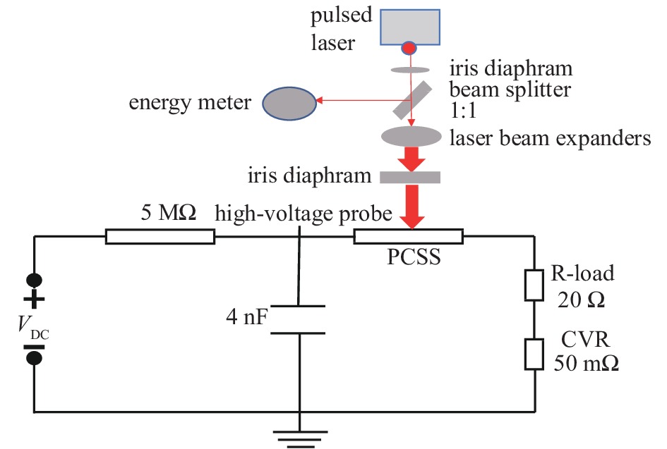
图 1 砷化镓光导开关结构示意图
Figure 1. Structural schematic diagram of GaAs photoconductive switch
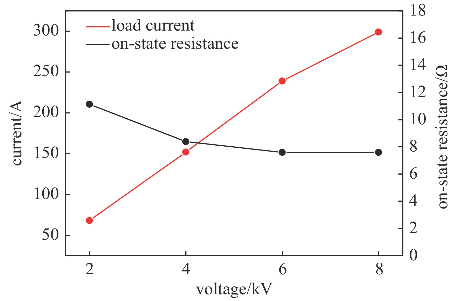
图 3 光导开关在不同偏置电压下的电流值及光导开关的最小导通电阻值
Figure 3. Current value of photoconductive switch under different bias voltage and minimum on-resistance value of photoconductive switch

图 4 光导开关在不同触发能量下的电流值及光导开关的最小导通电阻值
Figure 4. Current value of photoconductive switch at different triggering energies and minimum on-resistance value of photoconductive switch
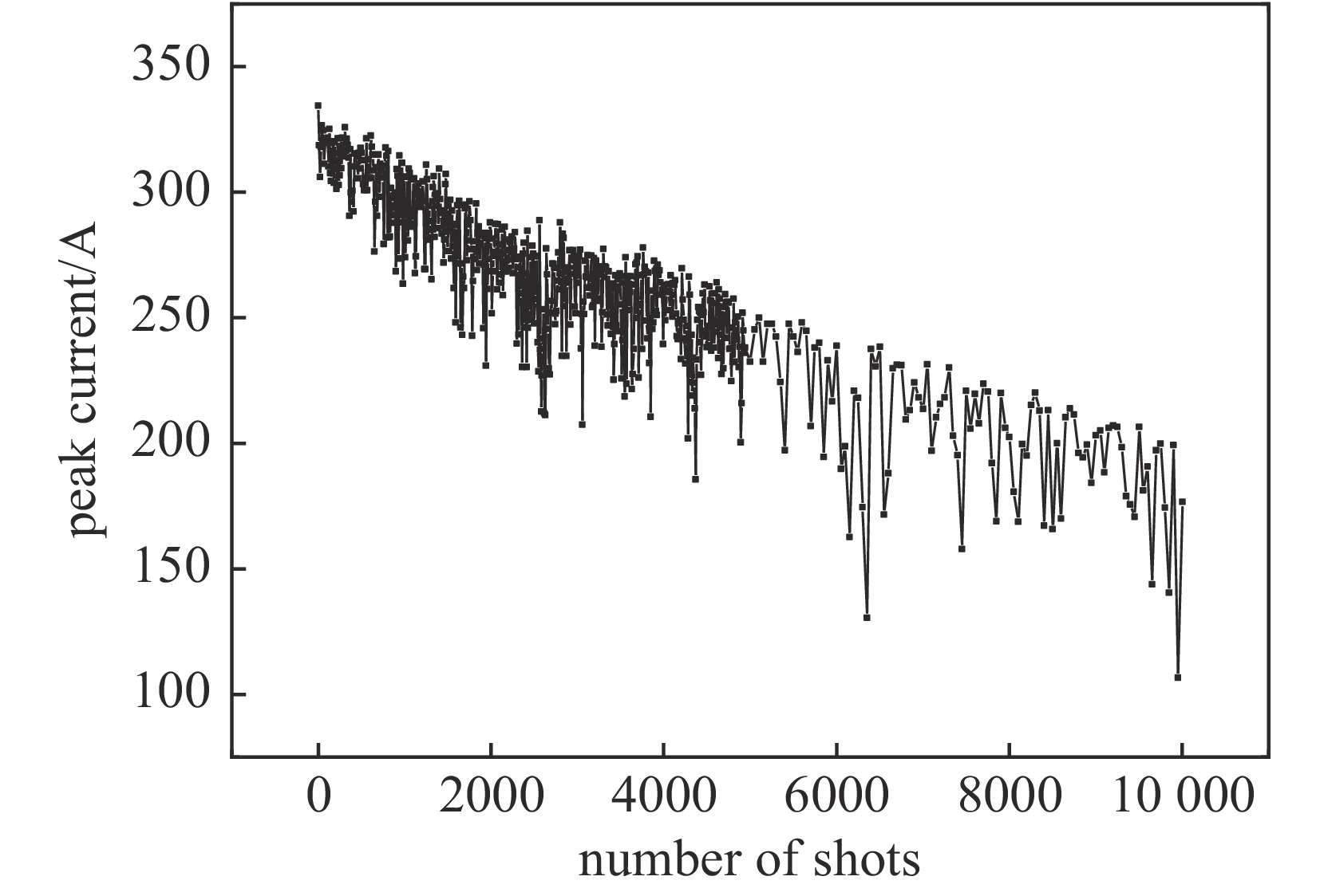
图 5 光导开关电流值与触发次数的关系图
Figure 5. Current value of photoconductive at different triggering number

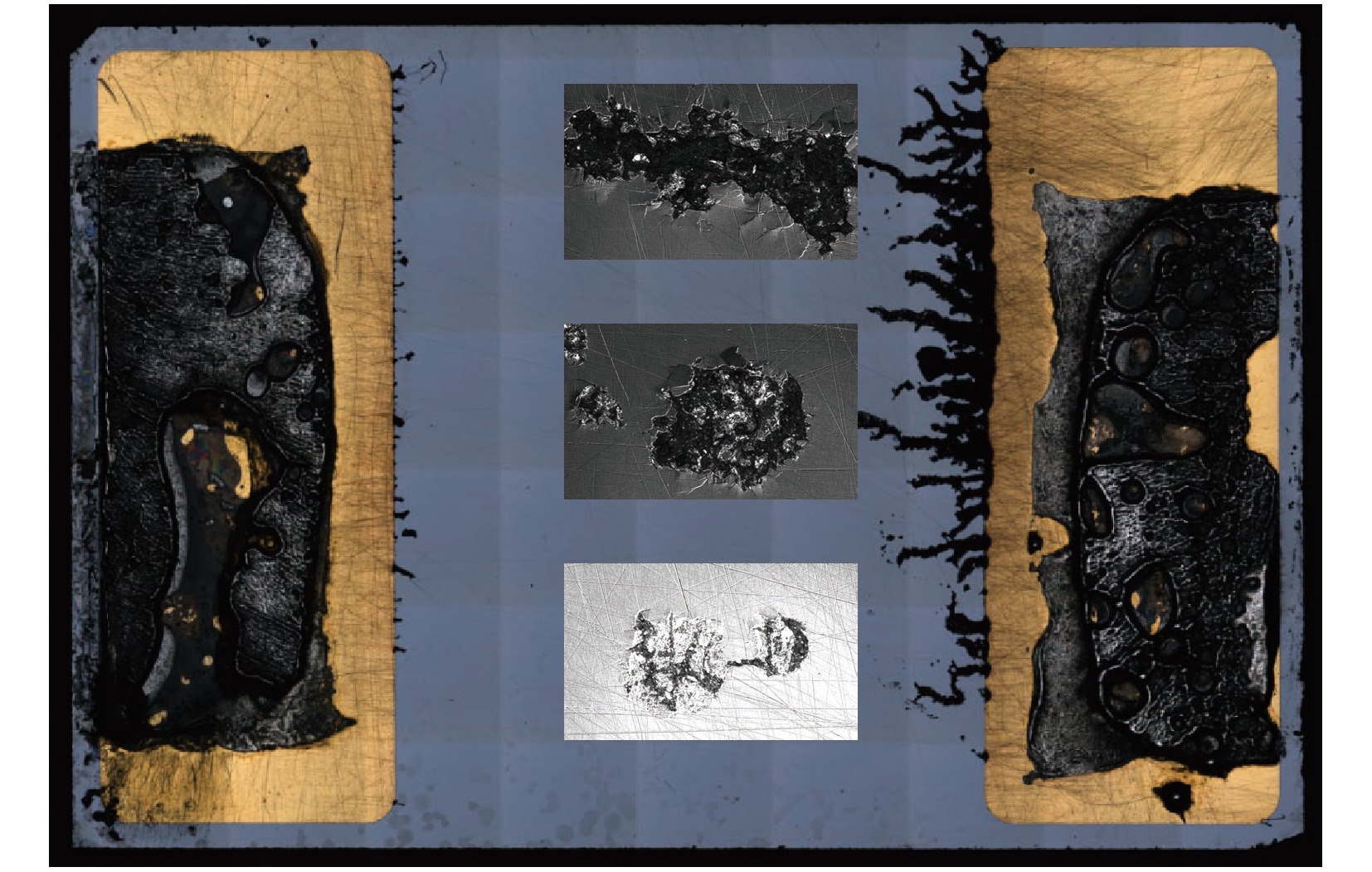
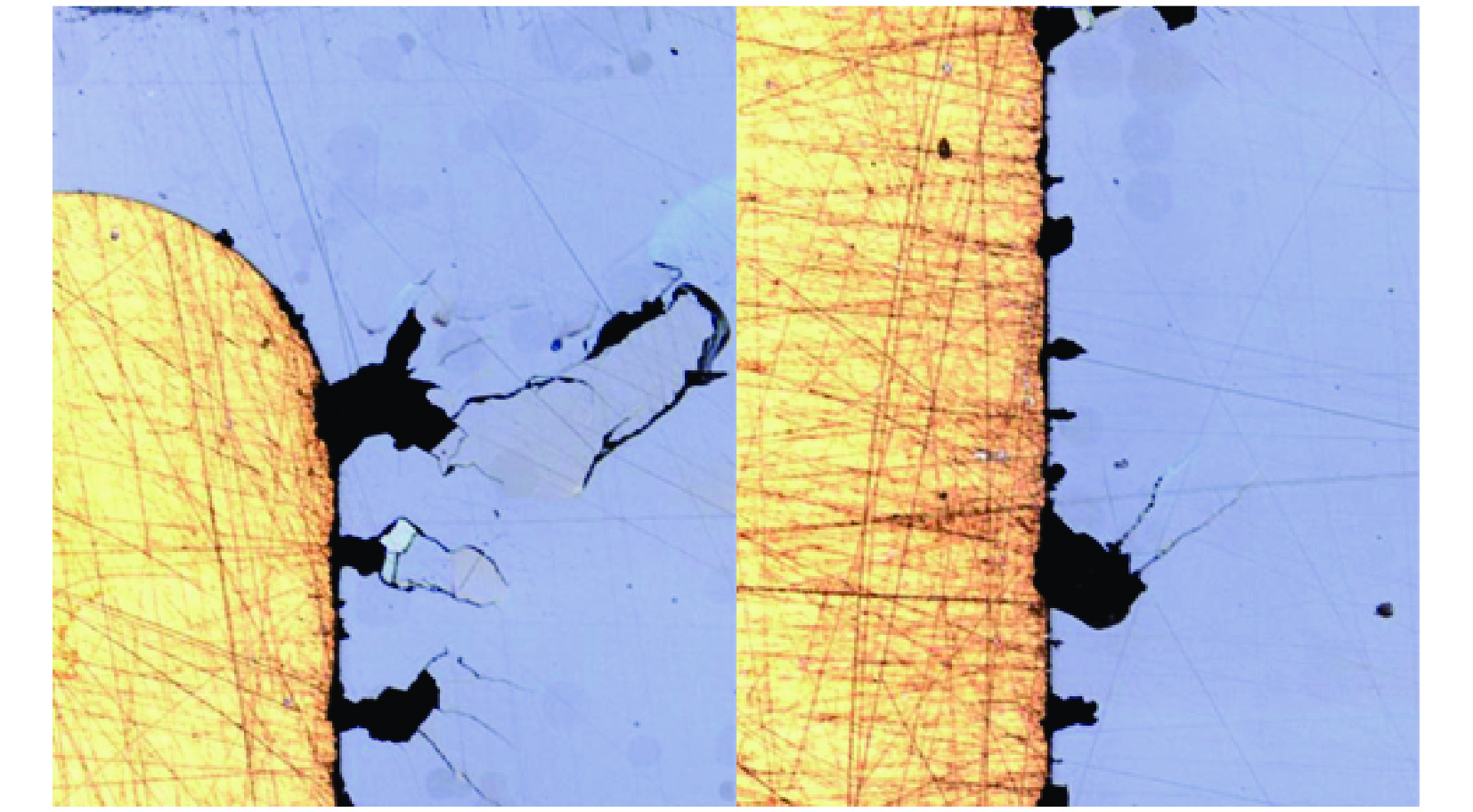
图 8 两个电极之间不同形式的损伤
Figure 8. Damage caused by thermal stress
(a), (b) single point injury; (c) diffuse point injury; (d) twin point injury; (e), (f) strip damage
-
[1] Shi Wei, Jiang Huan, Li Mengxia, et al. Investigation of electric field threshold of GaAs photoconductive semiconductor switch triggered by 1.6 μJ laser diode[J]. Applied Physics Letters, 2014, 104: 042108. doi: 10.1063/1.4863738 [2] Loubriel G M, Zutavern F J, Baca A G, et al. Photoconductive semiconductor switches[J]. IEEE Transactions on Plasma Science, 1997, 25(2): 124-130. doi: 10.1109/27.602482 [3] 施卫, 闫志巾. 雪崩倍增GaAs光电导太赫兹辐射源研究进展[J]. 物理学报, 2015, 64:228702. (Shi Wei, Yan Zhijin. Research progress on avalanche multiplication GaAs photoconductive terahertz emitter[J]. Acta Physica Sinica, 2015, 64: 228702 doi: 10.7498/aps.64.228702Shi Wei, Yan Zhijin. Research progress on avalanche multiplication GaAs photoconductive terahertz emitter[J]. Acta Physica Sinica, 2015, 64: 228702 doi: 10.7498/aps.64.228702 [4] Liu Xiaorong, Li Song. The effect of photoconductive semiconductor materials in improving the resolution of femtosecond streak camera[J]. IOP Conference Series: Materials Science and Engineering, 2020, 772: 012060. doi: 10.1088/1757-899X/772/1/012060 [5] Islam N E, Schamiloglu E, Fleddermann C B. Characterization of a semi-insulating GaAs photoconductive semiconductor switch for ultrawide band high power microwave applications[J]. Applied Physics Letters, 1998, 73(14): 1988-1990. doi: 10.1063/1.122344 [6] Mar A, Bacon L D, Loubriel G M. Device technology investigation: subsystems packaging study: feasibility of PCSS-based pulser for highly portable platforms[R]. SAND2002-2059, 2002: 2002-2059. [7] Glover S F, Zutavern F J, Swalby M E, et al. Pulsed- and DC-charged PCSS-based trigger generators[J]. IEEE Transactions on Plasma Science, 2010, 38(10): 2701-2707. doi: 10.1109/TPS.2010.2049662 [8] Nunnally W C. Critical component requirements for compact pulse power system architectures[J]. IEEE Transactions on Plasma Science, 2005, 33(4): 1262-1267. doi: 10.1109/TPS.2005.852406 [9] 严成锋, 施尔畏, 陈之战, 等. 超快大功率SiC光导开关的研究[J]. 无机材料学报, 2008, 23(3):425-428. (Yan Chengfeng, Shi Erwei, Chen Zhizhan, et al. Super fast and high power SiC photoconductive semiconductor switches[J]. Journal of Inorganic Materials, 2008, 23(3): 425-428 doi: 10.3321/j.issn:1000-324X.2008.03.002Yan Chengfeng, Shi Erwei, Chen Zhizhan, et al. Super fast and high power SiC photoconductive semiconductor switches[J]. Journal of Inorganic Materials, 2008, 23(3): 425-428 doi: 10.3321/j.issn:1000-324X.2008.03.002 [10] Tian Liqiang, Shi Wei, Feng Qingqing. Breakover mechanism of GaAs photoconductive switch triggering spark gap for high power applications[J]. Journal of Applied Physics, 2011, 110: 094507. doi: 10.1063/1.3658260 [11] Wang Langning, Jia Yongsheng, Liu Jinliang. Photoconductive semiconductor switch-based triggering with 1 ns jitter for trigatron[J]. Matter and Radiation at Extremes, 2018, 3(5): 256-260. doi: 10.1016/j.mre.2017.12.006 [12] Mar A, Loubriel G M, Zutavern F J, et al. Doped contacts for high-longevity optically activated, high-gain GaAs photoconductive semiconductor switches[J]. IEEE Transactions on Plasma Science, 2000, 28(5): 1507-1511. doi: 10.1109/27.901223 [13] Shi Wei, Ma Cheng, Li Mengxia. Research on the failure mechanism of high-power GaAs PCSS[J]. IEEE Transactions on Power Electronics, 2015, 30(5): 2427-2434. doi: 10.1109/TPEL.2014.2348493 [14] 刘宏伟, 袁建强, 刘金锋, 等. 大功率GaAs光导开关寿命实验研究[J]. 强激光与粒子束, 2010, 22(4):795-798. (Liu Hongwei, Yuan Jianqiang, Liu Jinfeng, et al. Experimental investigation on lifetime of high power GaAs photoconductive semiconductor switch[J]. High Power Laser and Particle Beams, 2010, 22(4): 795-798 doi: 10.3788/HPLPB20102204.0795Liu Hongwei, Yuan Jianqiang, Liu Jinfeng, et al. Experimental investigation on lifetime of high power GaAs photoconductive semiconductor switch[J]. High Power Laser and Particle Beams, 2010, 22(4): 795-798 doi: 10.3788/HPLPB20102204.0795 [15] 孙飞翔, 何晓雄, 常润发, 等. GaAs光导开关损伤机理研究[J]. 合肥工业大学学报(自然科学版), 2017, 40(4):497-501. (Sun Feixiang, He Xiaoxiong, Chang Runfa, et al. GaAs PCSS’s injuring mechanism[J]. Journal of Hefei University of Technology, 2017, 40(4): 497-501Sun Feixiang, He Xiaoxiong, Chang Runfa, et al. GaAs PCSS’s injuring mechanism[J]. Journal of Hefei University of Technology, 2017, 40(4): 497-501 [16] Hjalmarson H P, Kambour K, Myles C W, et al. Continuum models for electrical breakdown in photoconductive semiconductor switches[C]//16th IEEE International Pulsed Power Conference. 2007: 446-450. [17] Kambour K, Hjalmarson H P, Zutavern F J, et al. Simulation of current filaments in photoconductive semiconductor switches[C]//15th IEEE International Pulsed Power Conference. 2005: 814-817. [18] 张同意, 石顺祥, 赵卫, 等. 深能级杂质对光导半导体开关非线性特性的影响[J]. 光子学报, 2003, 31(1):121-123. (Zhang Tongyi, Shi Shunxiang, Zhao Wei, et al. The effect of deep level impurity on the nonlinear performances of photoconductive semiconductor switches[J]. Acta Photonica Sinica, 2003, 31(1): 121-123Zhang Tongyi, Shi Shunxiang, Zhao Wei, et al. The effect of deep level impurity on the nonlinear performances of photoconductive semiconductor switches[J]. Acta Photonica Sinica, 2003, 31(1): 121-123 [19] Brinkmann R P, Schoenbach K H, Mazzola M S, et al. Analysis of time-dependent current transport in an optically controlled Cu-compensated GaAs switch[C]//Proceedings of SPIE 1632, Optically Activated Switching II. 1992: 262-273. [20] 刘鸿, 阮成礼. 本征砷化镓光导开关中的流注模型[J]. 科学通报, 2008, 53(18):2181-2185. ((Liu Hong, Ruan Chengli. Flow model in intrinsic gallium arsenide photoconductive switch[J]. Chinese Science Bulletin, 2008, 53(18): 2181-2185 doi: 10.3321/j.issn:0023-074X.2008.18.005(Liu Hong, Ruan Chengli. Flow model in intrinsic gallium arsenide photoconductive switch[J]. Chinese Science Bulletin, 2008, 53(18): 2181-2185. doi: 10.3321/j.issn:0023-074X.2008.18.005 [21] Ma Cheng, Shi Wei, Li Mengxia, et al. Impact of current filaments on the material and output characteristics of GaAs Photoconductive Switches[J]. IEEE Transactions on Electron Device, 2014, 61(7): 2432-2436. doi: 10.1109/TED.2014.2323052 [22] Hu Long, Xu Ming, Li Xin, et al. Performance investigation of bulk photoconductive semiconductor switch based on reversely biased p+-i-n+ structure[J]. Transactions on Electron Devices, 2020, 67(11): 4963-4969. doi: 10.1109/TED.2020.3025984 [23] Ma Cheng, Shi Wei, Dong Chengang, et al. 998 multiplication rate of GaAs avalanche semiconductor switch triggered by 0.567 nJ[J]. IEEE Access, 2020, 8: 116515-116519. doi: 10.1109/ACCESS.2020.3004054 期刊类型引用(2)
1. 韩星,王永琴,曾娅秋,刘宇,粟嘉伟,林珑君. 双极晶体管空间辐射效应的研究进展. 环境技术. 2024(07): 188-194 .  百度学术
百度学术2. 曾超,许献国,钟乐. 抗辐射电子学研究综述. 太赫兹科学与电子信息学报. 2023(04): 452-471 . 百度学术其他类型引用(3)
-


 下载:
下载:


 下载:
下载:
 点击查看大图
计量
- 文章访问数: 911
- HTML全文浏览量: 231
- PDF下载量: 87
- 被引次数: 5
