

Effect of different nitrogen ion implantation parameters on surface charge accumulation and dissipation characteristics of polytetrafluoroethene
-
摘要: 为了有效抑制聚四氟乙烯(PTFE)材料表面电荷积聚、进一步提升其沿面耐压性能,采用射频产生氮等离子体对其表面进行等离子体浸没离子注入。注入过程中改变射频功率、脉宽、脉冲幅值等参数实现对PTFE样品表面的不同改性效果。通过测试其注入前后的X射线光电子能谱、表面形貌、表面电阻率、表面电位衰减特性、表面陷阱能级及其密度分布,较为系统地研究了不同注入参数对聚四氟乙烯样品表面成分、表面电荷积聚和消散特性的影响。结果表明:注入过程中,氮离子主要通过自身动能促使聚四氟乙烯材料表面分子结构发生破裂和重组来实现表面改性而并非通过化学反应引入新成分,注入氮离子的动能以及数量是决定表面改性效果的主要因素。随着射频源功率增加,射频源对氮气利用效率得到提升,其处理效果饱和点由100 W射频功率下的20 cm3/min升至400 W射频功率下的30 cm3/min,相应表面电阻率由100 W-10 cm3/min条件下的最大值
$ 3.3\times {10}^{16}\;\mathrm{\Omega }/\mathrm{m}{\mathrm{m}}^{2} $ 降至400 W-30 cm3/min条件下的最小值$ 1\times {10}^{15}\;\mathrm{\Omega }/\mathrm{m}{\mathrm{m}}^{2} $ ,并且表面电荷消散速度由6%增加至68%,同时积聚量最多减少了18.6%。另外,随着外施脉冲电压由3 kV-25 μs升至7 kV-75 μs,表面电阻率最多下降了89%,表面电荷消散速度由4%增加至58%,积聚量最多减少了23.7%。进一步分析表明,经氮离子注入处理的聚四氟乙烯材料表面陷阱能级变浅,加速了表面电荷脱陷,而降低的表面电阻率也促进了脱陷的表面电荷沿面传导,最终使得表面电荷消散加快。Abstract: To suppress the surface charge accumulation and improve the surface pressure resistance of polytetrafluoroethene (PTFE), the plasma immersion ion implantation was carried out on the surface of PTFE by radio frequency (RF) generation nitrogen plasma. The modification effect of PTFE sample surface was realized by changing RF power, pulse width and pulse amplitude during injection. X-ray photoelectron spectroscopy, surface morphology, surface resistivity, surface potential attenuation characteristics, surface trap energy level and density distribution were measured before and after injection. The effects of different injection parameters on surface composition, surface charge accumulation and dissipation characteristics of PTFE samples were systematically studied. The results show that nitrogen ions can achieve surface modification mainly through their own kinetic energy, rather than introducing new components through chemical reaction. The kinetic energy and quantity of nitrogen ions are the main factors determining the surface modification effect. With the increase of RF source power, nitrogen utilization efficiency of RF source is improved, the saturation point of treatment effect increases from 20 cm3/min at 100 W RF power to 30 cm3/min at 400 W RF power. The corresponding surface resistivity decreases from the maximum value$ 3.3\times {10}^{16}\;\mathrm{\Omega }/\mathrm{m}{\mathrm{m}}^{2} $ at 100 W-10 cm3/min to the minimum value$ 1\times {10}^{15}\;\mathrm{\Omega }/\mathrm{m}{\mathrm{m}}^{2} $ at 400 W-30 cm3/min, the surface charge dissipation rate increases from 6% to 68%. At the same time,the accumulation decreases by 18.6% at most. In addition, when the applied pulse voltage increases from 3 kV-25 μs to 7 kV-75 μs, The surface resistivity decreased by up to 89%, the surface charge dissipation rate increases from 4% to 58%, and the accumulation decreases by 23.7% at most. Further analysis shows that the trap energy level becomes shallow, which accelerates the surface charge debonding, and the reduced surface resistivity promotes the surface charge conduction along the surface of the debonding, and finally accelerates the surface charge dissipation. -
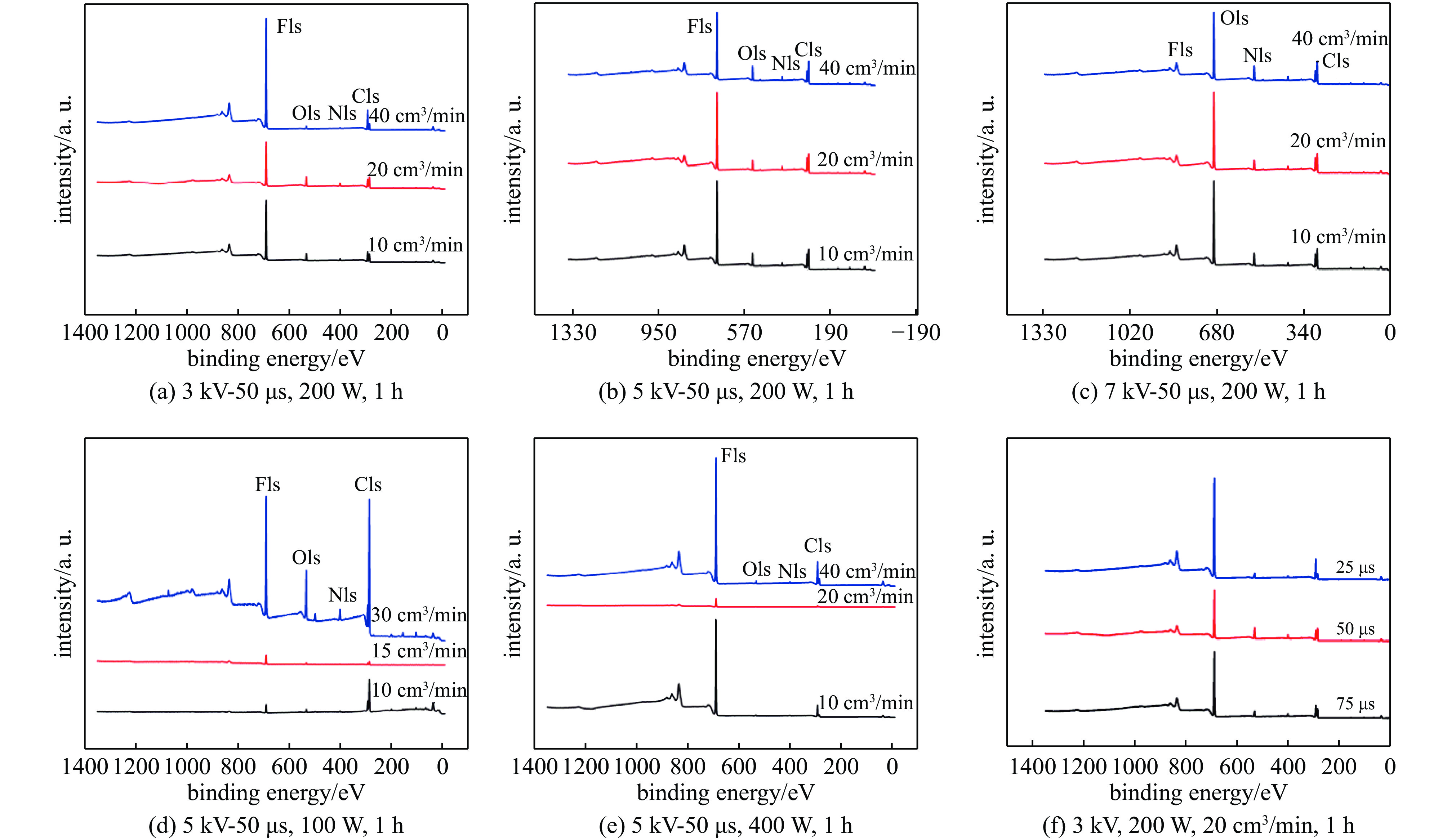
图 1 不同处理条件下的PTFE表面XPS全谱
Figure 1. Full spectrum of XPS on PTFE surface under different treatment conditions

图 2 不同脉冲电压与氮气流量处理下的PTFE表面XPS C谱
Figure 2. XPS C spectra of PTFE surface under different pulse voltage and nitrogen flow

图 3 不同脉冲宽度处理和射频功率下的PTFE表面XPS C谱
Figure 3. XPS C spectra of PTFE surface treated with different RF source power and pulse voltage widths
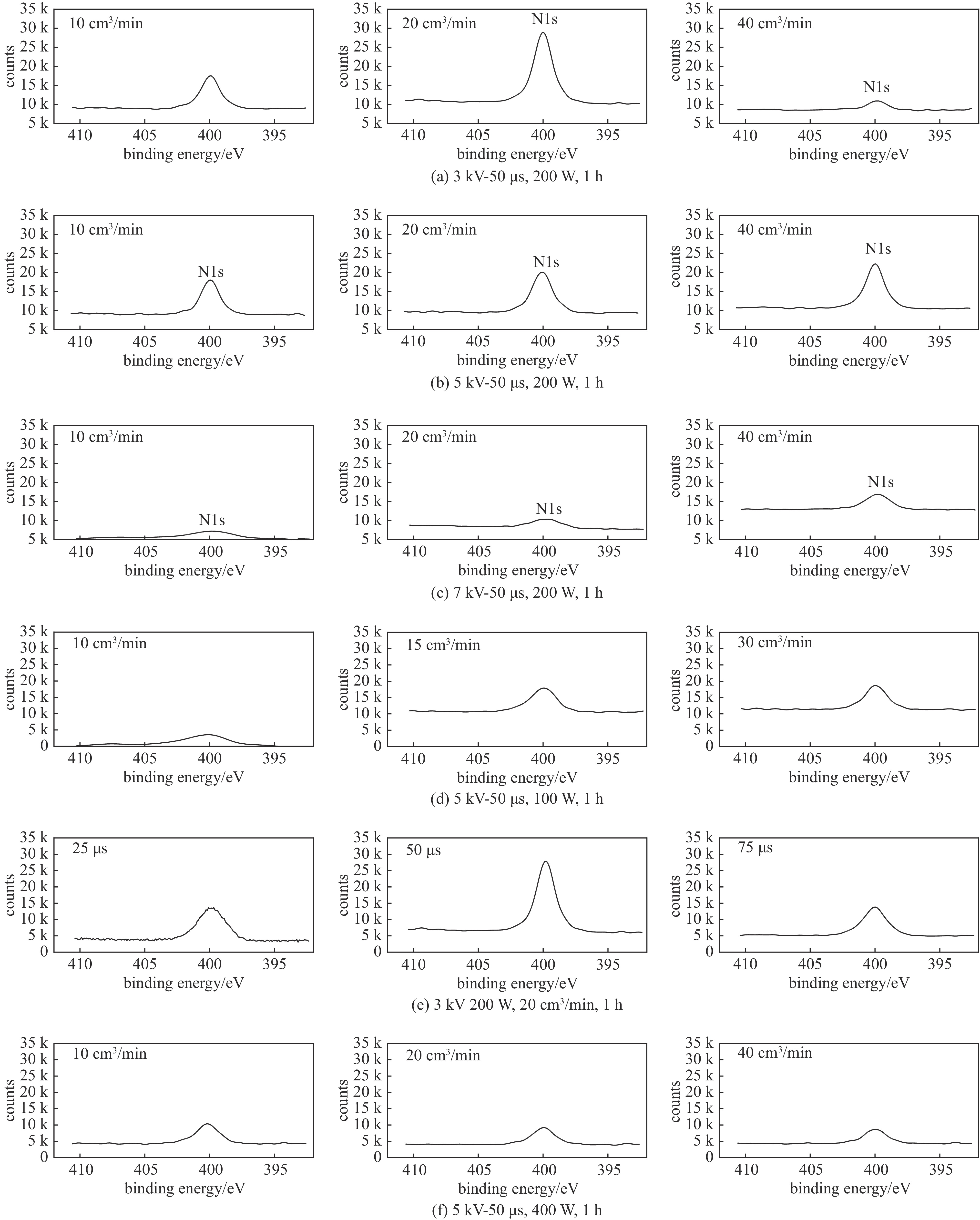
图 4 不同处理条件下的PTFE表面XPS N谱
Figure 4. XPS N spectra of PTFE surface under different treatment conditions

图 5 不同氮气流量处理下的PTFE表面形貌
Figure 5. Surface morphology of PTFE under different nitrogen flow treatments
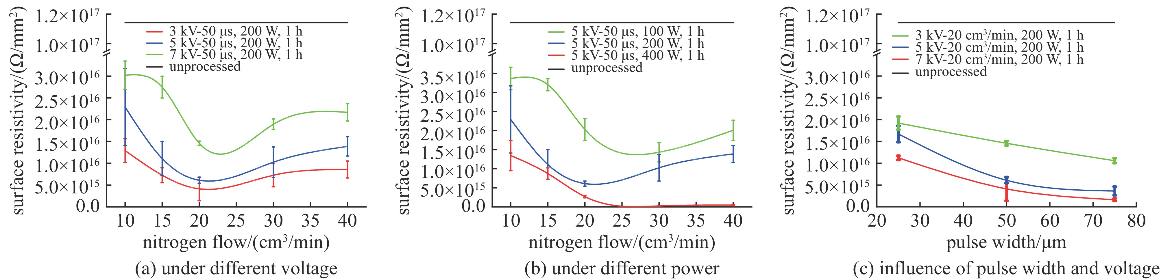
图 6 不同处理条件对PTFE样品表面电阻率的影响
Figure 6. Effect of different treatment conditions on the surface resistivity of PTFE samples

图 7 不同处理条件下的PTFE表面中心电位衰减特性
Figure 7. Attenuation characteristics of central potential on PTFE surface under different treatment conditions

图 8 不同处理条件下的PTFE表面陷阱分布特性
Figure 8. Distribution characteristics of traps on PTFE surface under different treatment conditions
表 1 实验样品的处理条件
Table 1. Treatment conditions of experimental samples
No. voltage/kV pulse width/μs power/W processed time/h nitrogen flow/(cm3·min−1) 1~5 3 50 200 1 10~40 6~10 5 50 200 1 10~40 11~15 7 50 200 1 10~40 16~17 3 25,75 200 1 20 18~9 5 25,75 200 1 20 20 7 25 200 1 20 21~25 5 50 100 1 10~30 26~29 5 50 400 1 10~40  下载: 导出CSV
表 2 离子注入处理前后PTFE样品表面C元素各状态所占比例
Table 2. Radicals and proportion of C elements in PTFE sample surface before and after ion implantation
sample number processing parameters proportion of C element/% CF3 CF2 CF C=O C−O CF3 1 3 kV-50 μs, 10 cm3/min, 200 W, 1 h 0.00 44.02 1.29 8.62 7.44 37.45 2 3 kV-50 μs, 20 cm3/min, 200 W, 1 h 1.36 25.90 1.05 11.65 14.17 42.38 3 3 kV-50 μs, 40 cm3/min, 200 W, 1 h 5.31 61.34 1.50 2.51 3.48 23.41 4 5 kV-50 μs, 10 cm3/min, 200 W, 1 h 0.85 26.14 0.40 8.09 9.00 53.73 5 5 kV-50 μs, 20 cm3/min, 200 W, 1 h 0.33 43.08 0.44 9.72 8.27 37.78 6 5 kV-50 μs, 40 cm3/min, 200 W, 1 h 1.32 23.05 0.13 8.81 9.06 62.07 7 7 kV-50 μs, 40 cm3/min, 200 W, 1 h 2.19 67.94 3.44 2.79 7.46 21.13 8 7 kV-50 μs, 20 cm3/min, 200 W, 1 h 1.61 63.03 2.68 4.75 5.01 21.69 9 7 kV-50 μs, 10 cm3/min3, 100 W, 1 h 2.17 57.36 5.34 7.60 6.55 25.69 10 3 kV-25 μs, 20 cm3/min, 100 W, 1 h 1.03 41.13 1.80 11.19 8.81 37.74 11 3 kV-50 μs, 20 cm3/min, 100 W, 1 h 2.10 59.95 1.94 9.26 8.62 16.33 12 5 kV-50 μs, 10 cm3/min, 100 W, 1 h 1.08 19.59 2.01 5.76 10.72 64.25 13 5 kV-50 μs, 20 cm3/min3, 100 W, 1 h 0 20.68 0.14 9.87 5.86 61.92 14 5 kV-50 μs, 40 cm3/min3, 100 W, 1 h 0.00 10.84 1.18 4.78 10.12 72.34 15 5 kV-50 μs, 10 cm3/min3, 400 W, 1 h 3.34 66.43 3.01 5.65 4.98 9.53 16 5 kV-50 μs, 20 cm3/min3, 400 W, 1 h 3.69 50.59 3.67 10.84 10.70 17.97 17 5 kV-50 μs, 40 cm3/min, 400 W, 1 h 4.97 61.31 2.32 7.93 3.93 19.92
下载: 导出CSV
-
[1] 谢苏江. 聚四氟乙烯的改性及应用[J]. 化工新型材料, 2002, 30(11):26-30 doi: 10.3969/j.issn.1006-3536.2002.11.007Xie Sujiang. Modifying of poly (tetrafluoroethylene) and its application[J]. New Chemical Materials, 2002, 30(11): 26-30 doi: 10.3969/j.issn.1006-3536.2002.11.007 [2] 汪沨, 邱毓昌, 张乔根, 等. 表面电荷积聚对绝缘子沿面闪络影响的研究[J]. 中国电力, 2002, 35(9):52-55 doi: 10.3969/j.issn.1004-9649.2002.09.014Wang Feng, Qiu Yuchang, Zhang Qiaogen, et al. Study on influence of surface charge accumulation on flashover of insulator[J]. Electric Power, 2002, 35(9): 52-55 doi: 10.3969/j.issn.1004-9649.2002.09.014 [3] Kumara S, Serdyuk Y V, Gubanski S M. Simulation of surface charge effect on impulse flashover characteristics of outdoor polymeric insulators[J]. IEEE Transactions on Dielectrics and Electrical Insulation, 2010, 17(6): 1754-1763. doi: 10.1109/TDEI.2010.5658226 [4] Kato K, Kato H, Ishida T, et al. Influence of surface charges on impulse flashover characteristics of alumina dielectrics in vacuum[J]. IEEE Transactions on Dielectrics and Electrical Insulation, 2009, 16(6): 1710-1716. doi: 10.1109/TDEI.2009.5361594 [5] Du B X, Xiao Meng. Influence of surface charge on DC flashover characteristics of epoxy/BN nanocomposites[J]. IEEE Transactions on Dielectrics and Electrical Insulation, 2014, 21(2): 529-536. doi: 10.1109/TDEI.2013.004137 [6] Yan Ping, Shao Tao, Wang Jue, et al. Experimental investigation of surface flashover in vacuum using nanosecond pulses[J]. IEEE Transactions on Dielectrics and Electrical Insulation, 2007, 14(3): 634-642. doi: 10.1109/TDEI.2007.369524 [7] Ma Guoming, Zhou Hongyang, Li Chengrong, et al. Designing epoxy insulators in SF6-filled DC-GIL with simulations of ionic conduction and surface charging[J]. IEEE Transactions on Dielectrics and Electrical Insulation, 2015, 22(6): 3312-3320. doi: 10.1109/TDEI.2015.005031 [8] Kindersberger J, Lederle C. Surface charge decay on insulators in air and sulfurhexafluorid—part I: simulation[J]. IEEE Transactions on Dielectrics and Electrical Insulation, 2008, 15(4): 941-948. doi: 10.1109/TDEI.2008.4591214 [9] Yamamoto O, Takuma T, Fukuda M, et al. Improving withstand voltage by roughening the surface of an insulating spacer used in vacuum[J]. IEEE Transactions on Dielectrics and Electrical Insulation, 2003, 10(4): 550-556. doi: 10.1109/TDEI.2003.1219636 [10] 郎艳, 王艺博, 苏国强, 等. 表面粗糙度对有机玻璃材料真空沿面闪络特性的影响[J]. 高电压技术, 2015, 41(2):474-478 doi: 10.13336/j.1003-6520.hve.2015.02.017Lang Yan, Wang Yibo, Su Guoqiang, et al. Influence of surface roughness on vacuum flashover characteristics of PMMA[J]. High Voltage Engineering, 2015, 41(2): 474-478 doi: 10.13336/j.1003-6520.hve.2015.02.017 [11] Guo Baohong, Sun Guangyu, Zhang Shu, et al. Mechanism of vacuum flashover on surface roughness[J]. Journal of Physics D: Applied Physics, 2019, 52: 215301. doi: 10.1088/1361-6463/ab05a0 [12] 吕金壮. 氧化铝陶瓷的陷阱分布对其真空中沿面闪络特性的影响[D]. 北京: 华北电力大学(北京), 2003: 66-74Lv Jinzhuang. The influence of trap distribution of alumina ceramics on the surface flashover performance in vacuum[D]. Beijing: North China Electric Power University (Beijing), 2003: 66-74 [13] Li Chengrong, Ding Lijian, Lv Jinzhuang, et al. The relation of trap distribution of alumina with surface flashover performance in vacuum[J]. IEEE Transactions on Dielectrics and Electrical Insulation, 2006, 13(1): 79-84. doi: 10.1109/TDEI.2006.1593404 [14] Li Shengtao, Huang Qifeng, Sun Jian, et al. Effect of traps on surface flashover of XLPE in vacuum[J]. IEEE Transactions on Dielectrics and Electrical Insulation, 2010, 17(3): 964-970. doi: 10.1109/TDEI.2010.5492273 [15] Fukuda H, Yamano Y, Kobayashi S, et al. Relationship between vacuum surface flashover and charging characteristics for alumina ceramics of lowered resistivity[C]//Proceedings of the 2013 2nd International Conference on Electric Power Equipment-Switching Technology. 2013: 1-4. [16] 王邸博, 唐炬, 陶加贵, 等. 直流电压下闪络及电晕后聚合物表面电荷积聚特性[J]. 高电压技术, 2015, 41(11):3618-3627 doi: 10.13336/j.1003-6520.hve.2015.11.014Wang Dibo, Tang Ju, Tao Jiagui, et al. Surface charge accumulation characteristics on polymer after flashover and corona charging under DC voltage[J]. High Voltage Engineering, 2015, 41(11): 3618-3627 doi: 10.13336/j.1003-6520.hve.2015.11.014 [17] 陈士修, 解广润. 温度对电晕特性的影响[J]. 高电压技术, 1994, 20(3):3-8 doi: 10.13336/j.1003-6520.hve.1994.03.002Chen Shixiu, Xie Guangrun. The effect of temperature on the corona performances[J]. High Voltage Engineering, 1994, 20(3): 3-8 doi: 10.13336/j.1003-6520.hve.1994.03.002 [18] Lutz B, Kindersberger J. Influence of the relative humidity on the DC potential distribution of polymeric cylindrical model insulators[C]//Proceedings of the 2010 International Conference on Condition Monitoring and Diagnosis. 2010: 541-544. [19] Zhang Guanjun, Su Guoqiang, Song Baipeng, et al. Pulsed flashover across a solid dielectric in vacuum[J]. IEEE Transactions on Dielectrics and Electrical Insulation, 2018, 25(6): 2321-2339. doi: 10.1109/TDEI.2018.007133 [20] Guo Baohong, Wang Yibo, Su Guoqiang, et al. Influence of surface modification by direct fluorination on dielectric flashover characteristics in vacuum[C]//Proceedings of the 2017 1st International Conference on Electrical Materials and Power Equipment. 2017: 552-555. [21] Duan Li, Liu Wenyuan, Ke Changfeng, et al. Significantly improved surface flashover characteristics of insulators in vacuum by direct fluorination[J]. Colloids and Surfaces A: Physicochemical and Engineering Aspects, 2014, 456: 1-9. [22] 柯昌凤, 刘文元, 段荔, 等. 表面改性对绝缘子真空沿面闪络特性的影响[J]. 强激光与粒子束, 2014, 26:065010 doi: 10.11884/HPLPB201426.065010Ke Changfeng, Liu Wenyuan, Duan Li, et al. Influence of surface modification on vacuum flashover performance of insulators[J]. High Power Laser and Particle Beams, 2014, 26: 065010 doi: 10.11884/HPLPB201426.065010 [23] Cross J D, Sudarshan T S. The effect of cuprous oxide coatings on surface flashover of dielectric spacers in vacuum[J]. IEEE Transactions on Electrical Insulation, 1974, EI-9(4): 146-150. doi: 10.1109/TEI.1974.299325 [24] Chen Sile, Wang Shuai, Wang Yibo, et al. Surface modification of epoxy resin using He/CF4 atmospheric pressure plasma jet for flashover withstanding characteristics improvement in vacuum[J]. Applied Surface Science, 2017, 414: 107-113. doi: 10.1016/j.apsusc.2017.03.278 [25] Zhang Cheng, Lin Haofan, Zhang Shuai, et al. Plasma surface treatment to improve surface charge accumulation and dissipation of epoxy resin exposed to DC and nanosecond-pulse voltages[J]. Journal of Physics D: Applied Physics, 2017, 50: 405203. doi: 10.1088/1361-6463/aa829b [26] 何佳龙, 杨振, 李杰, 等. 离子束辐照影响氧化铝陶瓷真空沿面闪络性能的初步研究[C]//中国核科学技术进展报告(第五卷). 2017: 22-27He Jialong, Yang Zhen, Li Jie, et al. Preliminary investigation on the influence of ion beam irradiation on vacuum surface flashover characteristics of alumina ceramic[C]//Progress Report on China Nuclear Science & Technology (Vol. 5). 2017: 22-27 [27] 汤宝寅, 王浪平. 等离子体浸泡式离子注入与沉积技术[M]. 北京: 国防工业出版社, 2012: 1-17Tang Baoyin, Wang Langping. Plasma immersion ion implantation and deposition technique[M]. Beijing: National Defense Industry Press, 2012: 1-17 [28] Zhu Mingdong, Song Falun, Li Fei, et al. Surface insulating properties of titanium implanted alumina ceramics by plasma immersion ion implantation[J]. Nuclear Instruments and Methods in Physics Research Section B: Beam Interactions with Materials and Atoms, 2017, 407: 155-159. -


 点击查看大图
计量
- 文章访问数: 946
- HTML全文浏览量: 321
- PDF下载量: 119
- 被引次数: 0
